SLVSES8A October 2020 – December 2020 LM5127-Q1
PRODUCTION DATA
- 1 Features
- 2 Applications
- 3 Description
- 4 Revision History
- 5 Description (continued)
- 6 Pin Configuration and Functions
- 7 Specifications
-
8 Detailed Description
- 8.1 Overview
- 8.2 Functional Block Diagram
- 8.3
Feature Description
- 8.3.1 Device Enable (EN, VCC_HOLD)
- 8.3.2 Dual Input VCC Regulator (BIAS, VCCX, VCC)
- 8.3.3 Dual Input VDD Switch (VDD, VDDX)
- 8.3.4 Device Configuration and Light Load Switching Mode Selection (CFG/MODE)
- 8.3.5 Fixed or Adjustable Output Regulation Target (VOUT, FB)
- 8.3.6 Overvoltage Protection (VOUT, FB)
- 8.3.7 Power Good Indicator (PGOOD)
- 8.3.8 Programmable Switching Frequency (RT)
- 8.3.9 External Clock Synchronization (SYNC)
- 8.3.10 Programmable Spread Spectrum (DITHER)
- 8.3.11 Programmable Soft Start (SS)
- 8.3.12 Fast Re-start using VCC_HOLD (VCC_HOLD)
- 8.3.13 Transconductance Error Amplifier and PWM (COMP)
- 8.3.14 Current Sensing and Slope Compensation (CSA, CSB)
- 8.3.15 Constant Peak Current Limit (CSA, CSB)
- 8.3.16 Maximum Duty Cycle and Minimum Controllable On-time Limits (Boost)
- 8.3.17 Bypass Mode (Boost)
- 8.3.18 Minimum Controllable On-time and Minimum Controllable Off-time Limits (Buck)
- 8.3.19 Low Dropout Mode for Extended Minimum Input Voltage (Buck)
- 8.3.20 Programmable Hiccup Mode Overload Protection (RES)
- 8.3.21 MOSFET Drivers and Hiccup Mode Fault Protection (LO, HO, HB)
- 8.3.22 Battery Monitor (BMOUT, BMIN_FIX, BMIN_PRG)
- 8.3.23 Dual-phase Interleaved Configuration for High Current Supply (CFG)
- 8.3.24 Thermal Shutdown Protection
- 8.3.25 External VCCX Supply Reduces Power Dissipation
- 8.4 Device Functional Modes
- 9 Application and Implementation
- 10Power Supply Recommendations
- 11Layout
- 12Device and Documentation Support
- 13Mechanical, Packaging, and Orderable Information
Package Options
Mechanical Data (Package|Pins)
- RGZ|48
Thermal pad, mechanical data (Package|Pins)
- RGZ|48
Orderable Information
8.3.22 Battery Monitor (BMOUT, BMIN_FIX, BMIN_PRG)
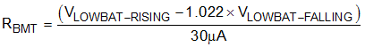
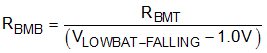
A battery monitor function is enabled when CH1 is configured as a buck, and at least one of the EN pins is greater than VEN or VCC_HOLD is greater than VSYNC. If BMIN_PRG is less than BMIN_PRG threshold (VSLEEP) and BMIN_FIX is greater than BMIN_FIX threshold (VBMIN_FIX), BMOUT is connected to AGND. BMOUT opens when BMIN_FIX is greater than VBMIN_FIX or BMIN_PRG is greater than VSLEEP. By using a resistor voltage divider at BMIN_PRG, the threshold of the battery monitor can be programmed, but the resistor divider and the internal 30-μA hysteresis current (ISLEEP1) will drain the battery.
 Figure 8-25 Battery Monitor
To adjust the low battery voltage detection levels, select the battery monitor resistor values as follows. The low battery falling detection level should be lower than 5.7 V and the low battery rising detection level should be higher than 6.0 V to program.