SNVSB29C October 2018 – June 2021 LM5143-Q1
PRODUCTION DATA
- 1 Features
- 2 Applications
- 3 Description
- 4 Revision History
- 5 Description (continued)
- 6 Pin Configuration and Functions
- 7 Specifications
-
8 Detailed Description
- 8.1 Overview
- 8.2 Functional Block Diagram
- 8.3
Feature Description
- 8.3.1 Input Voltage Range (VIN)
- 8.3.2 High-Voltage Bias Supply Regulator (VCC, VCCX, VDDA)
- 8.3.3 Enable (EN1, EN2)
- 8.3.4 Power Good Monitor (PG1, PG2)
- 8.3.5 Switching Frequency (RT)
- 8.3.6 Clock Synchronization (DEMB)
- 8.3.7 Synchronization Out (SYNCOUT)
- 8.3.8 Spread Spectrum Frequency Modulation (DITH)
- 8.3.9 Configurable Soft Start (SS1, SS2)
- 8.3.10 Output Voltage Setpoint (FB1, FB2)
- 8.3.11 Minimum Controllable On-Time
- 8.3.12 Error Amplifier and PWM Comparator (FB1, FB2, COMP1, COMP2)
- 8.3.13 Slope Compensation
- 8.3.14 Inductor Current Sense (CS1, VOUT1, CS2, VOUT2)
- 8.3.15 Hiccup Mode Current Limiting (RES)
- 8.3.16 High-Side and Low-Side Gate Drivers (HO1/2, LO1/2, HOL1/2, LOL1/2)
- 8.3.17 Output Configurations (MODE, FB2)
- 8.4 Device Functional Modes
-
9 Application and Implementation
- 9.1 Application Information
- 9.2 Typical Applications
- 10Power Supply Recommendations
- 11Layout
- 12Device and Documentation Support
- 13Mechanical, Packaging, and Orderable Information
Package Options
Mechanical Data (Package|Pins)
- RWG|40
Thermal pad, mechanical data (Package|Pins)
Orderable Information
3 Description
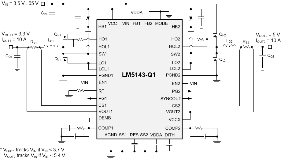
The LM5143-Q1 is a 65-V synchronous buck DC/DC controller for high-current single or dual outputs. The device uses an interleaved, stackable, peak current-mode control architecture for easy loop compensation, fast transient response, excellent load and line regulation, and accurate current sharing with paralleled phases for higher output current. A high-side switch minimum on-time of 65 ns gives large step-down ratios, enabling the direct conversion from 12-V, 24-V, or 48-Vautomotive inputs to low-voltage rails for reduced system complexity and solution cost. The LM5143-Q1 continues to operate during input voltage dips as low as 3.5 V, at nearly 100% duty cycle if needed.
Current is sensed using the inductor DCR for highest efficiency or an optional shunt resistor for high accuracy. The 15-μA no-load quiescent current with the output voltage in regulation extends operating run-time in battery-powered systems. Power the LM5143-Q1 from the output of the switching regulator or another available source for even lower input quiescent current and power loss.
| PART NUMBER | PACKAGE(1) | BODY SIZE (NOM) |
|---|---|---|
| LM5143-Q1 | VQFNP (40) | 6.00 mm × 6.00 mm |
 High-Efficiency Dual
Step-Down Regulator