SNVSB32B August 2018 – June 2021 LM5146-Q1
PRODUCTION DATA
- 1 Features
- 2 Applications
- 3 Description
- 4 Revision History
- 5 Description (continued)
- 6 Pin Configuration and Functions
- 7 Specifications
-
8 Detailed Description
- 8.1 Overview
- 8.2 Functional Block Diagram
- 8.3
Feature Description
- 8.3.1 Input Range (VIN)
- 8.3.2 Output Voltage Setpoint and Accuracy (FB)
- 8.3.3 High-Voltage Bias Supply Regulator (VCC)
- 8.3.4 Precision Enable (EN/UVLO)
- 8.3.5 Power Good Monitor (PGOOD)
- 8.3.6 Switching Frequency (RT, SYNCIN)
- 8.3.7 Configurable Soft Start (SS/TRK)
- 8.3.8 Voltage-Mode Control (COMP)
- 8.3.9 Gate Drivers (LO, HO)
- 8.3.10 Current Sensing and Overcurrent Protection (ILIM)
- 8.3.11 OCP Duty Cycle Limiter
- 8.4 Device Functional Modes
- 9 Application and Implementation
- 10Power Supply Recommendations
- 11Layout
- 12Device and Documentation Support
- 13Mechanical, Packaging, and Orderable Information
Package Options
Refer to the PDF data sheet for device specific package drawings
Mechanical Data (Package|Pins)
- RGY|20
Thermal pad, mechanical data (Package|Pins)
- RGY|20
Orderable Information
10 Power Supply Recommendations
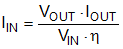
The LM5146-Q1 buck controller is designed to operate from a wide input voltage range from 5.5 V to 100 V. The characteristics of the input supply must be compatible with the Absolute Maximum Ratings and Recommended Operating Conditions. In addition, the input supply must be capable of delivering the required input current to the fully-loaded regulator. Estimate the average input current with Equation 23.
where
- η is the efficiency
If the converter is connected to an input supply through long wires or PCB traces with a large impedance, take special care to achieve stable performance. The parasitic inductance and resistance of the input cables may have an adverse affect on converter operation. The parasitic inductance in combination with the low-ESR ceramic input capacitors form an underdamped resonant circuit. This circuit can cause overvoltage transients at VIN each time the input supply is cycled ON and OFF. The parasitic resistance causes the input voltage to dip during a load transient. If the regulator is operating close to the minimum input voltage, this dip can cause false UVLO fault triggering and a system reset. The best way to solve such issues is to reduce the distance from the input supply to the regulator and use an aluminum or tantalum input capacitor in parallel with the ceramics. The moderate ESR of the electrolytic capacitors helps to damp the input resonant circuit and reduce any voltage overshoots. A capacitance in the range of 10 µF to 47 µF is usually sufficient to provide input damping and helps to hold the input voltage steady during large load transients.
An EMI input filter is often used in front of the regulator that, unless carefully designed, can lead to instability as well as some of the effects mentioned above. The application report Simple Success with Conducted EMI for DC-DC Converters (SNVA489) provides helpful suggestions when designing an input filter for any switching regulator.