SNVSAZ0C March 2018 – October 2021 LM51501-Q1
PRODUCTION DATA
- 1 Features
- 2 Applications
- 3 Description
- 4 Revision History
- 5 Device Comparison Table
- 6 Pin Configuration and Functions
- 7 Specifications
-
8 Detailed Description
- 8.1 Overview
- 8.2 Functional Block Diagram
- 8.3
Feature Description
- 8.3.1 Enable (EN Pin)
- 8.3.2 High Voltage VCC Regulator (PVCC, AVCC Pin)
- 8.3.3 Power-On Voltage Selection (VSET Pin)
- 8.3.4 Switching Frequency (RT Pin)
- 8.3.5 Clock Synchronization (SYNC Pin in SS Configuration)
- 8.3.6 Current Sense, Slope Compensation, and PWM (CS Pin)
- 8.3.7 Current Limit (CS Pin)
- 8.3.8 Feedback and Error Amplifier (COMP Pin)
- 8.3.9 Automatic Wake-Up and Standby
- 8.3.10 Boost Status Indicator (STATUS Pin)
- 8.3.11 Maximum Duty Cycle Limit and Minimum Input Supply Voltage
- 8.3.12 MOSFET Driver (LO Pin)
- 8.3.13 Thermal Shutdown
- 8.4 Device Functional Modes
-
9 Application and Implementation
- 9.1 Application Information
- 9.2
Typical Application
- 9.2.1 Design Requirements
- 9.2.2
Detailed Design Procedure
- 9.2.2.1 Custom Design With WEBENCH® Tools
- 9.2.2.2 RSET Resistor
- 9.2.2.3 RT Resistor
- 9.2.2.4 Inductor Selection (LM)
- 9.2.2.5 Current Sense (RS)
- 9.2.2.6 Slope Compensation Ramp (RSL)
- 9.2.2.7 Output Capacitor (COUT)
- 9.2.2.8 Loop Compensation Component Selection and Maximum ESR
- 9.2.2.9 PVCC Capacitor, AVCC Capacitor, and AVCC Resistor
- 9.2.2.10 VOUT Filter (CVOUT, RVOUT)
- 9.2.2.11 Input Capacitor
- 9.2.2.12 MOSFET Selection
- 9.2.2.13 Diode Selection
- 9.2.2.14 Efficiency Estimation
- 9.2.3 Application Curves
- 9.3 System Examples
- 10Power Supply Recommendations
- 11Layout
- 12Device and Documentation Support
- 13Mechanical, Packaging, and Orderable Information
Package Options
Refer to the PDF data sheet for device specific package drawings
Mechanical Data (Package|Pins)
- RUM|16
Thermal pad, mechanical data (Package|Pins)
- RUM|16
Orderable Information
9.2.2.14 Efficiency Estimation
The total loss of the boost converter (PTOTAL) can be expressed as the sum of the losses in the LM51501-Q1 (PIC), MOSFET power losses (PQ), diode power losses (PD), inductor power losses (PL), and the loss in the sense resistor (PRS).

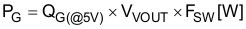
PIC can be separated into gate driving loss (PG) and the losses caused by quiescent current (PIQ) in Equation 42.

Each power loss is approximately calculated in Equation 43 and Equation 44:

IVIN and IVOUT values in each mode can be found in the supply current section of Section 7.5.
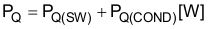
PQ can be separated into switching loss (PQ(SW)) and conduction loss (PQ(COND)) in Equation 45.
Each power loss is approximately calculated using Equation 46:

tR and tF are the rise and fall times of the low-side N-channel MOSFET device. ISUPPLY is the input supply current of the boost converter.
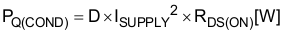
RDS(ON) is the on-resistance of the MOSFET and is specified in the MOSFET data sheet. Consider the RDS(ON) increase due to self-heating.
PD can be separated into diode conduction loss (PVF) and reverse recovery loss (PRR) in Equation 48.

Each power loss is approximately calculated using Equation 49 and Equation 50:


QRR is the reverse recovery charge of the diode and is specified in the diode data sheet. Remember that reverse recovery characteristics of the diode strongly affect efficiency, especially when the output voltage is high.
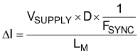
PL is the sum of DCR loss (PDCR) and AC core loss (PAC) in Equation 51. DCR is the DC resistance of inductor and is mentioned in the inductor data sheet.

Each power loss is approximately calculated by Equation 52, Equation 53, and Equation 54:


where
- ∆I is the peak-to-peak inductor current ripple.
- K, α, and β are core dependent factors that can be provided by the inductor manufacturer.
PRS is calculated as Equation 55:

Efficiency of the power converter can be estimated using Equation 56: