SNVSAY4F august 2018 – august 2023 LM5155-Q1 , LM51551-Q1
PRODUCTION DATA
- 1
- 1 Features
- 2 Applications
- 3 Description
- 4 Revision History
- 5 Description (continued)
- 6 Device Comparison Table
- 7 Pin Configuration and Functions
- 8 Specifications
-
9 Detailed Description
- 9.1 Overview
- 9.2 Functional Block Diagram
- 9.3
Feature Description
- 9.3.1 Line Undervoltage Lockout (UVLO/SYNC Pin)
- 9.3.2 High Voltage VCC Regulator (BIAS, VCC Pin)
- 9.3.3 Soft Start (SS Pin)
- 9.3.4 Switching Frequency (RT Pin)
- 9.3.5 Clock Synchronization (UVLO/SYNC Pin)
- 9.3.6 Current Sense and Slope Compensation (CS Pin)
- 9.3.7 Current Limit and Minimum On-time (CS Pin)
- 9.3.8 Feedback and Error Amplifier (FB, COMP Pin)
- 9.3.9 Power-Good Indicator (PGOOD Pin)
- 9.3.10 Hiccup Mode Overload Protection (LM51551 Only)
- 9.3.11 Maximum Duty Cycle Limit and Minimum Input Supply Voltage
- 9.3.12 MOSFET Driver (GATE Pin)
- 9.3.13 Overvoltage Protection (OVP)
- 9.3.14 Thermal Shutdown (TSD)
- 9.4 Device Functional Modes
- 10Application and Implementation
- 11Power Supply Recommendations
- 12Layout
- 13Device and Documentation Support
- 14Mechanical, Packaging, and Orderable Information
Package Options
Mechanical Data (Package|Pins)
- DSS|12
Thermal pad, mechanical data (Package|Pins)
- DSS|12
Orderable Information
9.3.4 Switching Frequency (RT Pin)
The switching frequency of the device can be set by a single RT resistor connected between the RT and the AGND pins. The resistor value to set the RT switching frequency (fRT) is calculated as shown in Equation 5.
Equation 5. 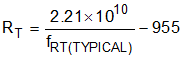
The RT pin is regulated to 0.5 V by the internal RT regulator when the device is enabled.