SNVSBI6 January 2021 LM5156 , LM51561
PRODUCTION DATA
- 1 Features
- 2 Applications
- 3 Description
- 4 Revision History
- 5 Description (continued)
- 6 Device Comparison Table
- 7 Pin Configuration and Functions
- 8 Specifications
-
9 Detailed Description
- 9.1 Overview
- 9.2 Functional Block Diagram
- 9.3
Feature Description
- 9.3.1 Line Undervoltage Lockout (UVLO/SYNC/EN Pin)
- 9.3.2 High Voltage VCC Regulator (BIAS, VCC Pin)
- 9.3.3 Soft Start (SS Pin)
- 9.3.4 Switching Frequency (RT Pin)
- 9.3.5 Dual Random Spread Spectrum (DRSS)
- 9.3.6 Clock Synchronization (UVLO/SYNC/EN Pin)
- 9.3.7 Current Sense and Slope Compensation (CS Pin)
- 9.3.8 Current Limit and Minimum On-time (CS Pin)
- 9.3.9 Feedback and Error Amplifier (FB, COMP Pin)
- 9.3.10 Power-Good Indicator (PGOOD pin)
- 9.3.11 Hiccup Mode Overload Protection (LM51561 Only)
- 9.3.12 Maximum Duty Cycle Limit and Minimum Input Supply Voltage
- 9.3.13 MOSFET Driver (GATE Pin)
- 9.3.14 Overvoltage Protection (OVP)
- 9.3.15 Thermal Shutdown (TSD)
- 9.4 Device Functional Modes
- 10Application and Implementation
- 11Power Supply Recommendations
- 12Layout
- 13Device and Documentation Support
- 14Mechanical, Packaging, and Orderable Information
Package Options
Mechanical Data (Package|Pins)
- DSS|12
Thermal pad, mechanical data (Package|Pins)
- DSS|12
Orderable Information
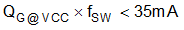
9.3.13 MOSFET Driver (GATE Pin)
The device provides an N-channel MOSFET driver that can source or sink a peak current of 1.5 A. The peak sourcing current is larger when supplying an external VCC that is higher than 6.75 V VCC regulation target. During start-up, especially when the input voltage range is below the VCC regulation target, the VCC voltage must be sufficient to completely enhance the MOSFET. If the MOSFET drive voltage is lower than the MOSFET gate plateau voltage during start-up, the boost converter may not start up properly and it can stick at the maximum duty cycle in a high power dissipation state. This condition can be avoided by selecting a lower threshold N-channel MOSFET switch and setting the VSUPPLY(ON) greater than 6 to 7 V. Because the internal VCC regulator has a limited sourcing capability, the MOSFET gate charge should satisfy the following inequality.
An internal 1-MΩ resistor is connected between GATE and GND to prevent a false turnon during shutdown. In boost topology, switch node dV/dT must be limited during the 65-µs internal start-up delay to avoid a false turnon, which is caused by the coupling through CDG parasitic capacitance of the MOSFET.