SNVSBT3 September 2020 LM51561H-Q1 , LM5156H-Q1
PRODUCTION DATA
- 1 Features
- 2 Applications
- 3 Description
- 4 Revision History
- 5 Description (continued)
- 6 Device Comparison Table
- 7 Pin Configuration and Functions
- 8 Specifications
-
9 Detailed Description
- 9.1 Overview
- 9.2 Functional Block Diagram
- 9.3
Feature Description
- 9.3.1 Line Undervoltage Lockout (UVLO/SYNC/EN Pin)
- 9.3.2 High Voltage VCC Regulator (BIAS, VCC Pin)
- 9.3.3 Soft Start (SS Pin)
- 9.3.4 Switching Frequency (RT Pin)
- 9.3.5 Dual Random Spread Spectrum (DRSS)
- 9.3.6 Clock Synchronization (UVLO/SYNC/EN Pin)
- 9.3.7 Current Sense and Slope Compensation (CS Pin)
- 9.3.8 Current Limit and Minimum On-time (CS Pin)
- 9.3.9 Feedback and Error Amplifier (FB, COMP Pin)
- 9.3.10 Power-Good Indicator (PGOOD Pin)
- 9.3.11 Hiccup Mode Overload Protection (LM51561H-Q1 Only)
- 9.3.12 Maximum Duty Cycle Limit and Minimum Input Supply Voltage
- 9.3.13 MOSFET Driver (GATE Pin)
- 9.3.14 Overvoltage Protection (OVP)
- 9.3.15 Thermal Shutdown (TSD)
- 9.4 Device Functional Modes
- 10Application and Implementation
- 11Power Supply Recommendations
- 12Layout
- 13Device and Documentation Support
- 14Mechanical, Packaging, and Orderable Information
Package Options
Mechanical Data (Package|Pins)
- PWP|14
Thermal pad, mechanical data (Package|Pins)
- PWP|14
Orderable Information
10.3.2.8 Efficiency Estimation
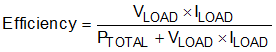
The total loss of the boost converter (PTOTAL) can be expressed as the sum of the losses in the device (PIC), MOSFET power losses (PQ), diode power losses (PD), inductor power losses (PL), and the loss in the sense resistor (PRS).

PIC can be separated into gate driving loss (PG) and the losses caused by quiescent current (PIQ).

Each power loss is approximately calculated as follows:


IVIN and IVOUT values in each mode can be found in the supply current section of Section 8.5.
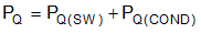
PQ can be separated into switching loss (PQ(SW)) and conduction loss (PQ(COND)).
Each power loss is approximately calculated as follows:

tR and tF are the rise and fall times of the low-side N-channel MOSFET device. ISUPPLY is the input supply current of the boost converter.

RDS(ON) is the on-resistance of the MOSFET and is specified in the MOSFET data sheet. Consider the RDS(ON) increase due to self-heating.
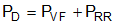
PD can be separated into diode conduction loss (PVF) and reverse recovery loss (PRR).
Each power loss is approximately calculated as follows:


QRR is the reverse recovery charge of the diode and is specified in the diode data sheet. Reverse recovery characteristics of the diode strongly affect efficiency, especially when the output voltage is high.
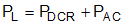
PL is the sum of DCR loss (PDCR) and AC core loss (PAC). DCR is the DC resistance of inductor which is mentioned in the inductor data sheet.
Each power loss is approximately calculated as follows:


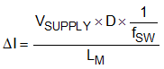
∆I is the peak-to-peak inductor current ripple. K, α, and β are core dependent factors which can be provided by the inductor manufacturer.
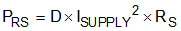
PRS is calculated as follows:
Efficiency of the power converter can be estimated as follows: