SNVSBK7A july 2021 – august 2023 LM5157
PRODUCTION DATA
- 1
- 1 Features
- 2 Applications
- 3 Description
- 4 Revision History
- 5 Device Comparison Table
- 6 Pin Configuration and Functions
- 7 Specifications
-
8 Detailed Description
- 8.1 Overview
- 8.2 Functional Block Diagram
- 8.3
Feature Description
- 8.3.1 Line Undervoltage Lockout (UVLO/SYNC/EN Pin)
- 8.3.2 High Voltage VCC Regulator (BIAS, VCC Pin)
- 8.3.3 Soft Start (SS Pin)
- 8.3.4 Switching Frequency (RT Pin)
- 8.3.5 Dual Random Spread Spectrum – DRSS (MODE Pin)
- 8.3.6 Clock Synchronization (UVLO/SYNC/EN Pin)
- 8.3.7 Current Sense and Slope Compensation
- 8.3.8 Current Limit and Minimum On Time
- 8.3.9 Feedback and Error Amplifier (FB, COMP Pin)
- 8.3.10 Power-Good Indicator (PGOOD Pin)
- 8.3.11 Hiccup Mode Overload Protection (MODE Pin)
- 8.3.12 Maximum Duty Cycle Limit and Minimum Input Supply Voltage
- 8.3.13 Internal MOSFET (SW Pin)
- 8.3.14 Overvoltage Protection (OVP)
- 8.3.15 Thermal Shutdown (TSD)
- 8.4 Device Functional Modes
- 9 Application and Implementation
- 10Power Supply Recommendations
- 11Layout
- 12Device and Documentation Support
- 13Mechanical, Packaging, and Orderable Information
Package Options
Mechanical Data (Package|Pins)
- RTE|16
Thermal pad, mechanical data (Package|Pins)
- RTE|16
Orderable Information
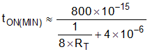
8.3.8 Current Limit and Minimum On Time
The device provides cycle-by-cycle peak current limit protection that turns off the internal MOSFET when the inductor current reaches the current limit threshold (ILIM). To avoid an unexpected Hiccup mode operation during a harsh load transient condition, it is recommended to have more margin when programming the peak-current limit.
Boost converters have a natural pass-through path from the supply to the load through the high-side power diode (D1). Because of this path and the minimum on-time limitation of the device, boost converters cannot provide current limit protection when the output voltage is close to or less than the input supply voltage. The minimum on time is is calculated as Equation 8.