SNVSBK8B october 2020 – august 2023 LM5157-Q1 , LM51571-Q1
PRODUCTION DATA
- 1
- 1 Features
- 2 Applications
- 3 Description
- 4 Revision History
- 5 Description (continued)
- 6 Device Comparison Table
- 7 Pin Configuration and Functions
- 8 Specifications
-
9 Detailed Description
- 9.1 Overview
- 9.2 Functional Block Diagram
- 9.3
Feature Description
- 9.3.1 Line Undervoltage Lockout (UVLO/SYNC/EN Pin)
- 9.3.2 High Voltage VCC Regulator (BIAS, VCC Pin)
- 9.3.3 Soft Start (SS Pin)
- 9.3.4 Switching Frequency (RT Pin)
- 9.3.5 Dual Random Spread Spectrum – DRSS (MODE Pin)
- 9.3.6 Clock Synchronization (UVLO/SYNC/EN Pin)
- 9.3.7 Current Sense and Slope Compensation
- 9.3.8 Current Limit and Minimum On Time
- 9.3.9 Feedback and Error Amplifier (FB, COMP Pin)
- 9.3.10 Power-Good Indicator (PGOOD Pin)
- 9.3.11 Hiccup Mode Overload Protection (MODE Pin)
- 9.3.12 Maximum Duty Cycle Limit and Minimum Input Supply Voltage
- 9.3.13 Internal MOSFET (SW Pin)
- 9.3.14 Overvoltage Protection (OVP)
- 9.3.15 Thermal Shutdown (TSD)
- 9.4 Device Functional Modes
- 10Application and Implementation
- 11Power Supply Recommendations
- 12Layout
- 13Device and Documentation Support
- 14Mechanical, Packaging, and Orderable Information
Package Options
Mechanical Data (Package|Pins)
- RTE|16
Thermal pad, mechanical data (Package|Pins)
- RTE|16
Orderable Information
9.3.12 Maximum Duty Cycle Limit and Minimum Input Supply Voltage
The practical duty cycle is greater than the estimated due to voltage drops across the MOSFET and sense resistor. The estimated duty cycle is calculated as shown in Equation 10.
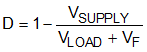
When designing boost converters, the maximum required duty cycle must be reviewed at the minimum supply voltage. The minimum input supply voltage that can achieve the target output voltage is limited by the maximum duty cycle limit, and it can be estimated as follows:

where
- ISUPPLY(MAX) is the maximum input current
- RDCR is the DC resistance of the inductor
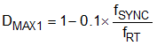

The minimum input supply voltage can be further decreased by supplying fSYNC, which is less than fRT. Practical DMAX is DMAX1 or DMAX2, whichever is lower.