SNVSBK8B october 2020 – august 2023 LM5157-Q1 , LM51571-Q1
PRODUCTION DATA
- 1
- 1 Features
- 2 Applications
- 3 Description
- 4 Revision History
- 5 Description (continued)
- 6 Device Comparison Table
- 7 Pin Configuration and Functions
- 8 Specifications
-
9 Detailed Description
- 9.1 Overview
- 9.2 Functional Block Diagram
- 9.3
Feature Description
- 9.3.1 Line Undervoltage Lockout (UVLO/SYNC/EN Pin)
- 9.3.2 High Voltage VCC Regulator (BIAS, VCC Pin)
- 9.3.3 Soft Start (SS Pin)
- 9.3.4 Switching Frequency (RT Pin)
- 9.3.5 Dual Random Spread Spectrum – DRSS (MODE Pin)
- 9.3.6 Clock Synchronization (UVLO/SYNC/EN Pin)
- 9.3.7 Current Sense and Slope Compensation
- 9.3.8 Current Limit and Minimum On Time
- 9.3.9 Feedback and Error Amplifier (FB, COMP Pin)
- 9.3.10 Power-Good Indicator (PGOOD Pin)
- 9.3.11 Hiccup Mode Overload Protection (MODE Pin)
- 9.3.12 Maximum Duty Cycle Limit and Minimum Input Supply Voltage
- 9.3.13 Internal MOSFET (SW Pin)
- 9.3.14 Overvoltage Protection (OVP)
- 9.3.15 Thermal Shutdown (TSD)
- 9.4 Device Functional Modes
- 10Application and Implementation
- 11Power Supply Recommendations
- 12Layout
- 13Device and Documentation Support
- 14Mechanical, Packaging, and Orderable Information
Package Options
Mechanical Data (Package|Pins)
- RTE|16
Thermal pad, mechanical data (Package|Pins)
- RTE|16
Orderable Information
9.3.3 Soft Start (SS Pin)
The soft-start feature helps the converter gradually reach the steady state operating point, thus reducing start-up stresses and surges. The device regulates the FB pin to the SS pin voltage or the internal reference, whichever is lower.
At start-up, the internal 10-μA soft-start current source (ISS) turns on after the VCC voltage exceeds the VCC UV threshold. The soft-start current gradually increases the voltage on an external soft-start capacitor connected to the SS pin. This results in a gradual rise of the output voltage. The SS pin is pulled down to ground by an internal switch when the VCC is less than VCC UVLO threshold, the UVLO is less than the UVLO threshold, during Hiccup mode off time or thermal shutdown.
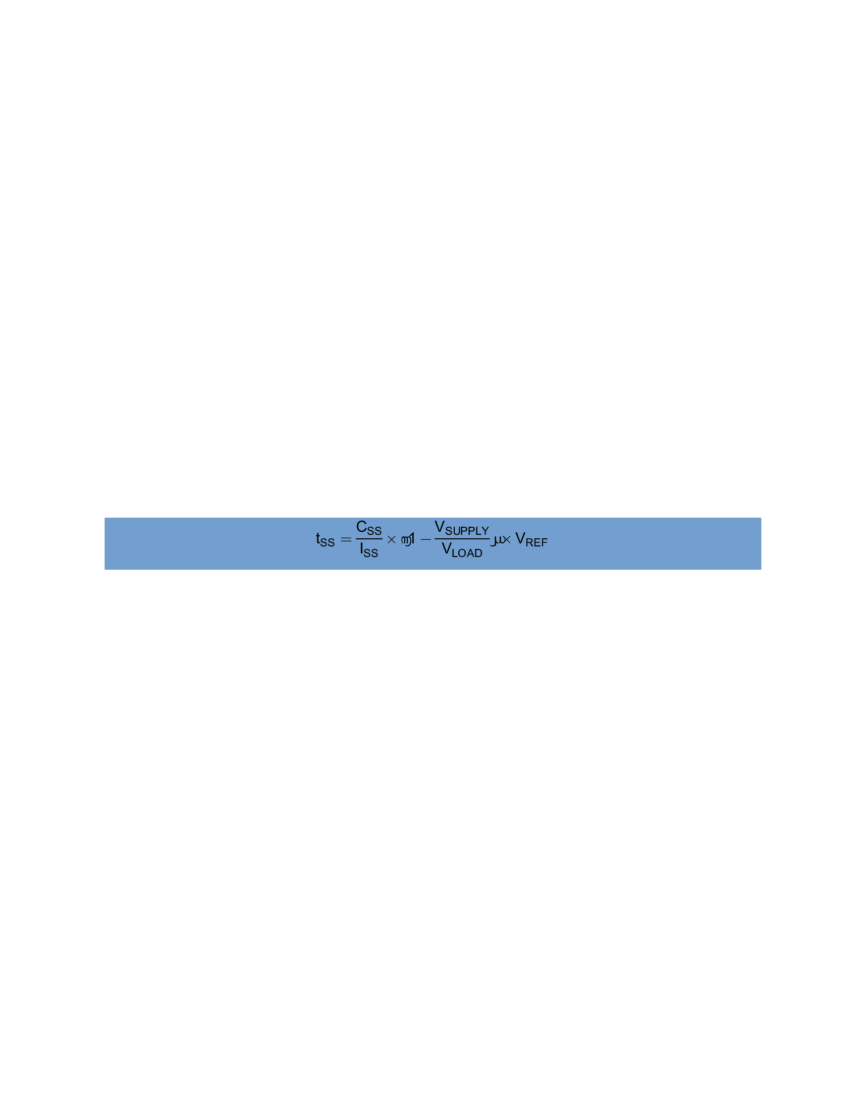
In boost topology, soft-start time (tSS) varies with the input supply voltage. The soft-start time in boost topology is calculated as shown in Equation 3.
In SEPIC topology, the soft-start time (tSS) is calculated as follows.
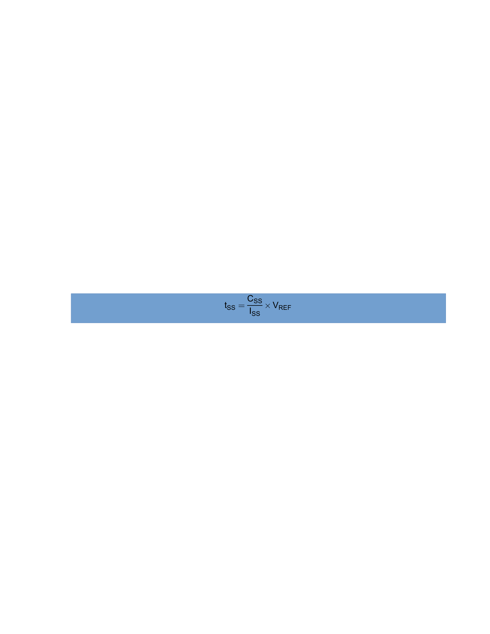
TI recommends choosing the soft-start time long enough so that the converter can start up without going into an overcurrent state. See Section 9.3.11 for more detailed information.
Figure 9-7 shows an implementation of primary side soft start in flyback topology.
 Figure 9-7 Primary-Side Soft Start in Flyback
Figure 9-8 shows an implementation of secondary side soft-start in flyback topology.
 Figure 9-8 Secondary-Side Soft Start in Flyback