SNVSBZ7 October 2021 LM5158 , LM51581
PRODUCTION DATA
- 1 Features
- 2 Applications
- 3 Description
- 4 Revision History
- 5 Description (continued)
- 6 Device Comparison Table
- 7 Pin Configuration and Functions
- 8 Specifications
-
9 Detailed Description
- 9.1 Overview
- 9.2 Functional Block Diagram
- 9.3
Feature Description
- 9.3.1 Line Undervoltage Lockout (EN/UVLO/SYNC Pin)
- 9.3.2 High Voltage VCC Regulator (BIAS, VCC Pin)
- 9.3.3 Soft Start (SS Pin)
- 9.3.4 Switching Frequency (RT Pin)
- 9.3.5 Dual Random Spread Spectrum – DRSS (MODE Pin)
- 9.3.6 Clock Synchronization (EN/UVLO/SYNC Pin)
- 9.3.7 Current Sense and Slope Compensation
- 9.3.8 Current Limit and Minimum On Time
- 9.3.9 Feedback and Error Amplifier (FB, COMP Pin)
- 9.3.10 Power-Good Indicator (PGOOD Pin)
- 9.3.11 Hiccup Mode Overload Protection (MODE Pin)
- 9.3.12 Maximum Duty Cycle Limit and Minimum Input Supply Voltage
- 9.3.13 Internal MOSFET (SW Pin)
- 9.3.14 Overvoltage Protection (OVP)
- 9.3.15 Thermal Shutdown (TSD)
- 9.4 Device Functional Modes
- 10Application and Implementation
- 11Power Supply Recommendations
- 12Layout
- 13Device and Documentation Support
- 14Mechanical, Packaging, and Orderable Information
Package Options
Mechanical Data (Package|Pins)
- RTE|16
Thermal pad, mechanical data (Package|Pins)
- RTE|16
Orderable Information
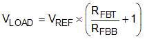
9.3.9 Feedback and Error Amplifier (FB, COMP Pin)
The feedback resistor divider is connected to an internal transconductance error amplifier, which features high output resistance (RO = 10 MΩ) and wide bandwidth (BW = 7 MHz). The internal transconductance error amplifier sources current, which is proportional to the difference between the FB pin and the SS pin voltage or the internal reference, whichever is lower. The internal transconductance error amplifier provides symmetrical sourcing and sinking capability during normal operation and reduces its sinking capability when the FB is greater than OVP threshold.
To set the output regulation target, select the feedback resistor values as shown in Equation 9.
The output of the error amplifier is connected to the COMP pin, allowing the use of a Type 2 loop compensation network. RCOMP, CCOMP, and optional CHF loop compensation components configure the error amplifier gain and phase characteristics to achieve a stable loop response. The absolute maximum voltage rating of the FB pin is 4.0 V. If necessary, the feedback resistor divider input can be clamped by using an external Zener diode.
The COMP pin features internal clamps. The maximum COMP clamp limits the maximum COMP pin voltage below its absolute maximum rating even in shutdown. The minimum COMP clamp limits the minimum COMP pin voltage in order to start switching as soon as possible during no load to heavy load transition. The minimum COMP clamp is disabled when FB is connected to ground in flyback topology.