SNVSAE4C July 2015 – October 2018 LM5160-Q1
PRODUCTION DATA.
- 1 Features
- 2 Applications
- 3 Description
- 4 Revision History
- 5 Pin Configuration and Functions
- 6 Specifications
- 7 Detailed Description
-
8 Application and Implementation
- 8.1 Application Information
- 8.2
Typical Applications
- 8.2.1
LM5160-Q1 Synchronous Buck (10-V to 60-V Input, 5-V Output, 1.5-A Load)
- 8.2.1.1 Design Requirements
- 8.2.1.2
Detailed Design Procedure
- 8.2.1.2.1 Custom Design With WEBENCH® Tools
- 8.2.1.2.2 Feedback Resistor Divider - RFB1, RFB2
- 8.2.1.2.3 Switching Frequency - RON
- 8.2.1.2.4 Inductor - L
- 8.2.1.2.5 Output Capacitor - COUT
- 8.2.1.2.6 Series Ripple Resistor - RESR
- 8.2.1.2.7 VCC and Bootstrap Capacitors - CVCC, CBST
- 8.2.1.2.8 Input Capacitor - CIN
- 8.2.1.2.9 Soft-Start Capacitor - CSS
- 8.2.1.2.10 EN/UVLO Resistors - RUV1, RUV2
- 8.2.1.3 Application Curves
- 8.2.2 LM5160-Q1 Isolated Fly-Buck (18-V to 32-V Input, 12-V, 4.5-W Isolated Output)
- 8.2.1
LM5160-Q1 Synchronous Buck (10-V to 60-V Input, 5-V Output, 1.5-A Load)
- 8.3 Do's and Don'ts
- 9 Power Supply Recommendations
- 10Layout
- 11Device and Documentation Support
- 12Mechanical, Packaging, and Orderable Information
Package Options
Mechanical Data (Package|Pins)
- PWP|14
Thermal pad, mechanical data (Package|Pins)
- PWP|14
Orderable Information
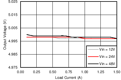
8.2.1.3 Application Curves
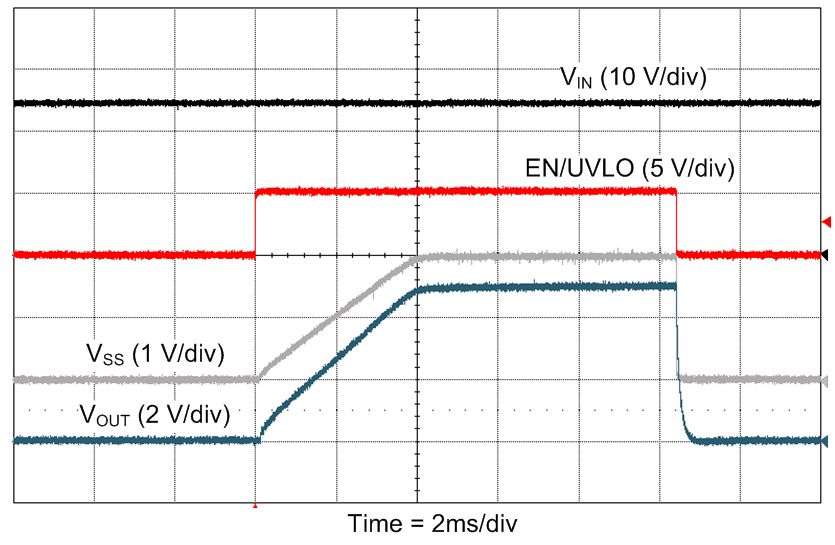 Figure 22. EN/UVLO Start-Up at VIN= 24 V and IOUT = 1 A
 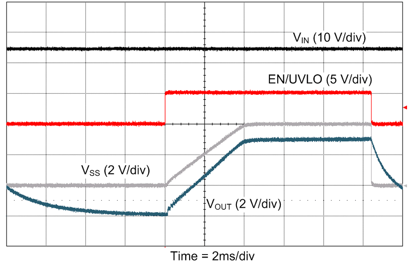 Figure 24. EN/UVLO Start-Up at VIN= 24 V and
RLOAD = 100 Ω
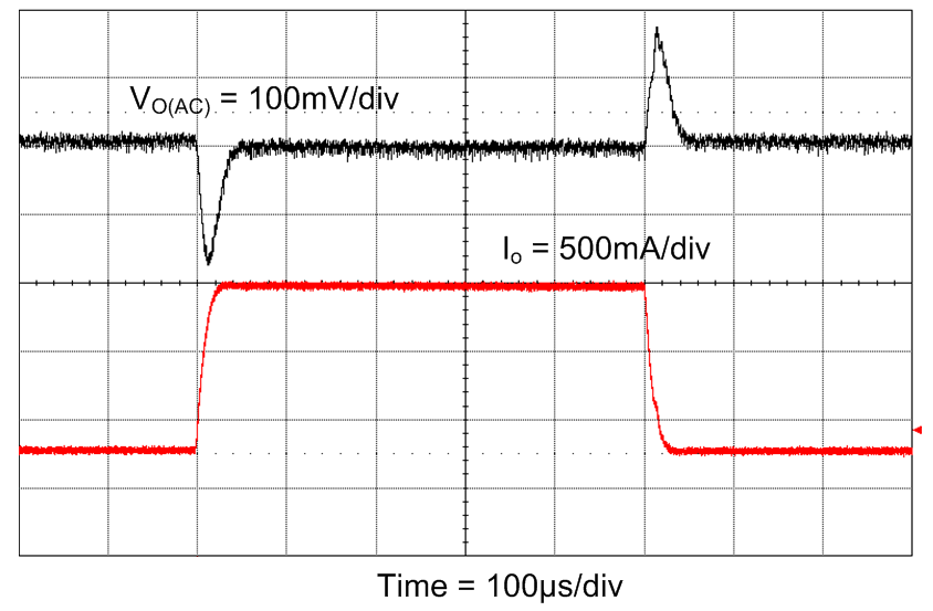 Figure 26. Load Transient (300 mA – 1.5 A) at VIN = 24 V With Type 3 Ripple Configuration
 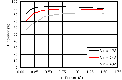 Figure 21. Efficiency vs IOUT
 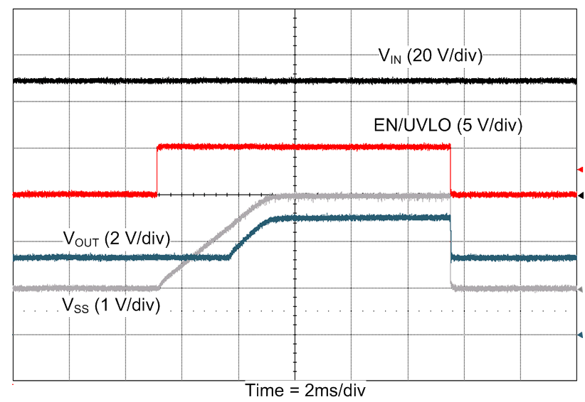 Figure 23. Prebias Start-Up at VIN= 48 V and RLOAD = 3 Ω
 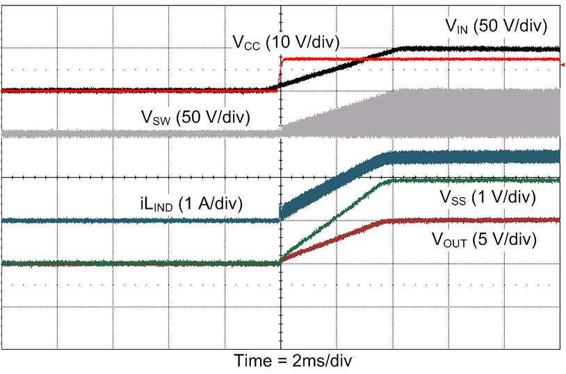 Figure 25. Start-Up at VIN= 48 V and RLOAD = 10 Ω
 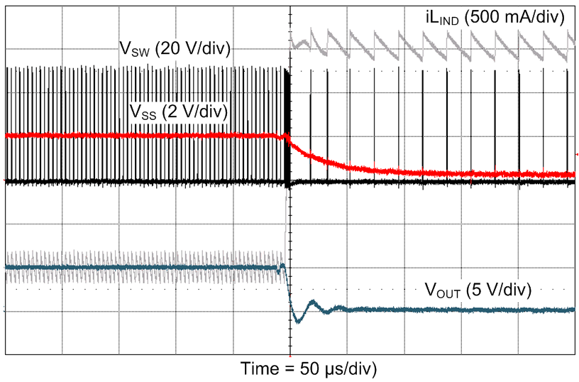 Figure 27. Output Short-Circuit at VIN = 48 V