SNVSA47D February   2016  – December 2022 LM5165

PRODUCTION DATA  

  1. Features
  2. Applications
  3. Description
  4. Revision History
  5. Pin Configuration and Functions
  6. Specifications
    1. 6.1 Absolute Maximum Ratings
    2. 6.2 ESD Ratings
    3. 6.3 Recommended Operating Conditions
    4. 6.4 Thermal Information
    5. 6.5 Electrical Characteristics
    6. 6.6 Switching Characteristics
    7. 6.7 Typical Characteristics
  7. Detailed Description
    1. 7.1 Overview
    2. 7.2 Functional Block Diagram
    3. 7.3 Feature Description
      1. 7.3.1  Integrated Power MOSFETs
      2. 7.3.2  Selectable PFM or COT Mode Converter Operation
      3. 7.3.3  COT Mode Light-Load Operation
      4. 7.3.4  Low Dropout Operation and 100% Duty Cycle Mode
      5. 7.3.5  Adjustable Output Voltage (FB)
      6. 7.3.6  Adjustable Current Limit
      7. 7.3.7  Precision Enable (EN) and Hysteresis (HYS)
      8. 7.3.8  Power Good (PGOOD)
      9. 7.3.9  Configurable Soft Start (SS)
      10. 7.3.10 Thermal Shutdown
    4. 7.4 Device Functional Modes
      1. 7.4.1 Shutdown Mode
      2. 7.4.2 Standby Mode
      3. 7.4.3 Active Mode in COT
      4. 7.4.4 Active Mode in PFM
      5. 7.4.5 Sleep Mode in PFM
  8. Applications and Implementation
    1. 8.1 Application Information
    2. 8.2 Typical Applications
      1. 8.2.1 Design 1: Wide VIN, Low IQ COT Converter Rated at 5 V, 150 mA
        1. 8.2.1.1 Design Requirements
        2. 8.2.1.2 Detailed Design Procedure
          1. 8.2.1.2.1 Custom Design With WEBENCH® Tools
          2. 8.2.1.2.2 Switching Frequency – RT
          3. 8.2.1.2.3 Filter Inductor – LF
          4. 8.2.1.2.4 Output Capacitors – COUT
          5. 8.2.1.2.5 Series Ripple Resistor – RESR
          6. 8.2.1.2.6 Input Capacitor – CIN
          7. 8.2.1.2.7 Soft-Start Capacitor – CSS
        3. 8.2.1.3 Application Curves
      2. 8.2.2 Design 2: Small Solution Size PFM Converter Rated at 3.3 V, 50 mA
        1. 8.2.2.1 Design Requirements
        2. 8.2.2.2 Detailed Design Procedure
          1. 8.2.2.2.1 Peak Current Limit Setting – RILIM
          2. 8.2.2.2.2 Switching Frequency – LF
          3. 8.2.2.2.3 Output Capacitor – COUT
          4. 8.2.2.2.4 Input Capacitor – CIN
        3. 8.2.2.3 Application Curves
      3. 8.2.3 Design 3: High Density 12-V, 75-mA PFM Converter
        1. 8.2.3.1 Design Requirements
        2. 8.2.3.2 Detailed Design Procedure
          1. 8.2.3.2.1 Peak Current Limit Setting – RILIM
          2. 8.2.3.2.2 Switching Frequency – LF
          3. 8.2.3.2.3 Input and Output Capacitors – CIN, COUT
          4. 8.2.3.2.4 Feedback Resistors – RFB1, RFB2
          5. 8.2.3.2.5 Undervoltage Lockout Setpoint – RUV1, RUV2, RHYS
          6. 8.2.3.2.6 Soft Start – CSS
        3. 8.2.3.3 Application Curves
      4. 8.2.4 Design 4: 3.3-V, 150-mA COT Converter With High Efficiency
        1. 8.2.4.1 Design Requirements
        2. 8.2.4.2 Application Curves
      5. 8.2.5 Design 5: 15-V, 150-mA, 600-kHz COT Converter
        1. 8.2.5.1 Design Requirements
        2. 8.2.5.2 Detailed Design Procedure
          1. 8.2.5.2.1 COT Output Ripple Voltage Reduction
        3. 8.2.5.3 Application Curves
    3. 8.3 Power Supply Recommendations
    4. 8.4 Layout
      1. 8.4.1 Layout Guidelines
        1. 8.4.1.1 Compact PCB Layout for EMI Reduction
        2. 8.4.1.2 Feedback Resistor Layout
      2. 8.4.2 Layout Example
  9. Device and Documentation Support
    1. 9.1 Device Support
      1. 9.1.1 Third-Party Products Disclaimer
      2. 9.1.2 Development Support
      3. 9.1.3 Custom Design With WEBENCH® Tools
    2. 9.2 Documentation Support
      1. 9.2.1 Related Documentation
    3. 9.3 Receiving Notification of Documentation Updates
    4. 9.4 Support Resources
    5. 9.5 Trademarks
    6. 9.6 Electrostatic Discharge Caution
    7. 9.7 Glossary
  10. 10Mechanical, Packaging, and Orderable Information

Package Options

Mechanical Data (Package|Pins)
Thermal pad, mechanical data (Package|Pins)
Orderable Information
Input Capacitor – CIN

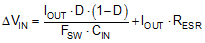
An input capacitor is necessary to limit the input ripple voltage while providing switching-frequency AC current to the buck power stage. To minimize the parasitic inductance in the switching loop, position the input capacitors as close as possible to the VIN and GND pins of the LM5165. The input capacitors conduct a square-wave current of peak-to-peak amplitude equal to the output current. It follows that the resultant capacitive component of AC ripple voltage is a triangular waveform. Together with the ESR-related ripple component, the peak-to-peak ripple voltage amplitude is given by Equation 17.

Equation 17. GUID-DFF4C210-D4A2-48C5-8153-A3BFB8B9C57E-low.gif

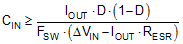
The input capacitance required for a particular load current, based on an input voltage ripple specification of ΔVIN, is given by Equation 18.

Equation 18. GUID-6D99C314-CA60-4EB1-B4BD-D452CEBD920B-low.gif

The recommended high-frequency capacitance is 1 µF or higher and must be a high-quality ceramic type X5R or X7R with sufficient voltage rating. Based on the voltage coefficient of ceramic capacitors, choose a voltage rating of twice the maximum input voltage. Additionally, some bulk capacitance is required if the LM5165 circuit is not located within approximately 5 cm from the input voltage source. This capacitor provides damping to the resonance associated with parasitic inductance of the supply lines and high-Q ceramics.