SNVSA47D February   2016  – December 2022 LM5165

PRODUCTION DATA  

  1. Features
  2. Applications
  3. Description
  4. Revision History
  5. Pin Configuration and Functions
  6. Specifications
    1. 6.1 Absolute Maximum Ratings
    2. 6.2 ESD Ratings
    3. 6.3 Recommended Operating Conditions
    4. 6.4 Thermal Information
    5. 6.5 Electrical Characteristics
    6. 6.6 Switching Characteristics
    7. 6.7 Typical Characteristics
  7. Detailed Description
    1. 7.1 Overview
    2. 7.2 Functional Block Diagram
    3. 7.3 Feature Description
      1. 7.3.1  Integrated Power MOSFETs
      2. 7.3.2  Selectable PFM or COT Mode Converter Operation
      3. 7.3.3  COT Mode Light-Load Operation
      4. 7.3.4  Low Dropout Operation and 100% Duty Cycle Mode
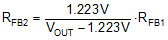
      5. 7.3.5  Adjustable Output Voltage (FB)
      6. 7.3.6  Adjustable Current Limit
      7. 7.3.7  Precision Enable (EN) and Hysteresis (HYS)
      8. 7.3.8  Power Good (PGOOD)
      9. 7.3.9  Configurable Soft Start (SS)
      10. 7.3.10 Thermal Shutdown
    4. 7.4 Device Functional Modes
      1. 7.4.1 Shutdown Mode
      2. 7.4.2 Standby Mode
      3. 7.4.3 Active Mode in COT
      4. 7.4.4 Active Mode in PFM
      5. 7.4.5 Sleep Mode in PFM
  8. Applications and Implementation
    1. 8.1 Application Information
    2. 8.2 Typical Applications
      1. 8.2.1 Design 1: Wide VIN, Low IQ COT Converter Rated at 5 V, 150 mA
        1. 8.2.1.1 Design Requirements
        2. 8.2.1.2 Detailed Design Procedure
          1. 8.2.1.2.1 Custom Design With WEBENCH® Tools
          2. 8.2.1.2.2 Switching Frequency – RT
          3. 8.2.1.2.3 Filter Inductor – LF
          4. 8.2.1.2.4 Output Capacitors – COUT
          5. 8.2.1.2.5 Series Ripple Resistor – RESR
          6. 8.2.1.2.6 Input Capacitor – CIN
          7. 8.2.1.2.7 Soft-Start Capacitor – CSS
        3. 8.2.1.3 Application Curves
      2. 8.2.2 Design 2: Small Solution Size PFM Converter Rated at 3.3 V, 50 mA
        1. 8.2.2.1 Design Requirements
        2. 8.2.2.2 Detailed Design Procedure
          1. 8.2.2.2.1 Peak Current Limit Setting – RILIM
          2. 8.2.2.2.2 Switching Frequency – LF
          3. 8.2.2.2.3 Output Capacitor – COUT
          4. 8.2.2.2.4 Input Capacitor – CIN
        3. 8.2.2.3 Application Curves
      3. 8.2.3 Design 3: High Density 12-V, 75-mA PFM Converter
        1. 8.2.3.1 Design Requirements
        2. 8.2.3.2 Detailed Design Procedure
          1. 8.2.3.2.1 Peak Current Limit Setting – RILIM
          2. 8.2.3.2.2 Switching Frequency – LF
          3. 8.2.3.2.3 Input and Output Capacitors – CIN, COUT
          4. 8.2.3.2.4 Feedback Resistors – RFB1, RFB2
          5. 8.2.3.2.5 Undervoltage Lockout Setpoint – RUV1, RUV2, RHYS
          6. 8.2.3.2.6 Soft Start – CSS
        3. 8.2.3.3 Application Curves
      4. 8.2.4 Design 4: 3.3-V, 150-mA COT Converter With High Efficiency
        1. 8.2.4.1 Design Requirements
        2. 8.2.4.2 Application Curves
      5. 8.2.5 Design 5: 15-V, 150-mA, 600-kHz COT Converter
        1. 8.2.5.1 Design Requirements
        2. 8.2.5.2 Detailed Design Procedure
          1. 8.2.5.2.1 COT Output Ripple Voltage Reduction
        3. 8.2.5.3 Application Curves
    3. 8.3 Power Supply Recommendations
    4. 8.4 Layout
      1. 8.4.1 Layout Guidelines
        1. 8.4.1.1 Compact PCB Layout for EMI Reduction
        2. 8.4.1.2 Feedback Resistor Layout
      2. 8.4.2 Layout Example
  9. Device and Documentation Support
    1. 9.1 Device Support
      1. 9.1.1 Third-Party Products Disclaimer
      2. 9.1.2 Development Support
      3. 9.1.3 Custom Design With WEBENCH® Tools
    2. 9.2 Documentation Support
      1. 9.2.1 Related Documentation
    3. 9.3 Receiving Notification of Documentation Updates
    4. 9.4 Support Resources
    5. 9.5 Trademarks
    6. 9.6 Electrostatic Discharge Caution
    7. 9.7 Glossary
  10. 10Mechanical, Packaging, and Orderable Information

Package Options

Mechanical Data (Package|Pins)
Thermal pad, mechanical data (Package|Pins)
Orderable Information

Adjustable Output Voltage (FB)

Three voltage feedback options are available: the fixed 3.3-V and 5-V versions include internal feedback resistors that sense the output directly through the VOUT pin; the adjustable voltage option senses the output through an external resistor divider connected from the output to the FB pin.

The LM5165 voltage regulation loop regulates the output voltage by maintaining the FB voltage equal to the internal reference voltage, VREF1. A resistor divider programs the ratio from output voltage VOUT to FB. For a target VOUT setpoint, calculate RFB2 based on the selected RFB1 using Equation 5.

Equation 5. GUID-91E44831-09B1-42C5-A667-AAE52ADE0ED6-low.gif

Selecting RFB1 in the range of 100 kΩ to 1 MΩ is recommended for most applications. A larger RFB1 consumes less DC current, which is mandatory if light-load efficiency is critical. However, RFB1 larger than 1 MΩ is not recommended as the feedback path becomes more susceptible to noise. High feedback resistances generally require more careful feedback path PCB layout. It is important to route the feedback trace away from the noisy area of the PCB. For more layout recommendations, see Layout.