SNVSA47D February   2016  – December 2022 LM5165

PRODUCTION DATA  

  1. Features
  2. Applications
  3. Description
  4. Revision History
  5. Pin Configuration and Functions
  6. Specifications
    1. 6.1 Absolute Maximum Ratings
    2. 6.2 ESD Ratings
    3. 6.3 Recommended Operating Conditions
    4. 6.4 Thermal Information
    5. 6.5 Electrical Characteristics
    6. 6.6 Switching Characteristics
    7. 6.7 Typical Characteristics
  7. Detailed Description
    1. 7.1 Overview
    2. 7.2 Functional Block Diagram
    3. 7.3 Feature Description
      1. 7.3.1  Integrated Power MOSFETs
      2. 7.3.2  Selectable PFM or COT Mode Converter Operation
      3. 7.3.3  COT Mode Light-Load Operation
      4. 7.3.4  Low Dropout Operation and 100% Duty Cycle Mode
      5. 7.3.5  Adjustable Output Voltage (FB)
      6. 7.3.6  Adjustable Current Limit
      7. 7.3.7  Precision Enable (EN) and Hysteresis (HYS)
      8. 7.3.8  Power Good (PGOOD)
      9. 7.3.9  Configurable Soft Start (SS)
      10. 7.3.10 Thermal Shutdown
    4. 7.4 Device Functional Modes
      1. 7.4.1 Shutdown Mode
      2. 7.4.2 Standby Mode
      3. 7.4.3 Active Mode in COT
      4. 7.4.4 Active Mode in PFM
      5. 7.4.5 Sleep Mode in PFM
  8. Applications and Implementation
    1. 8.1 Application Information
    2. 8.2 Typical Applications
      1. 8.2.1 Design 1: Wide VIN, Low IQ COT Converter Rated at 5 V, 150 mA
        1. 8.2.1.1 Design Requirements
        2. 8.2.1.2 Detailed Design Procedure
          1. 8.2.1.2.1 Custom Design With WEBENCH® Tools
          2. 8.2.1.2.2 Switching Frequency – RT
          3. 8.2.1.2.3 Filter Inductor – LF
          4. 8.2.1.2.4 Output Capacitors – COUT
          5. 8.2.1.2.5 Series Ripple Resistor – RESR
          6. 8.2.1.2.6 Input Capacitor – CIN
          7. 8.2.1.2.7 Soft-Start Capacitor – CSS
        3. 8.2.1.3 Application Curves
      2. 8.2.2 Design 2: Small Solution Size PFM Converter Rated at 3.3 V, 50 mA
        1. 8.2.2.1 Design Requirements
        2. 8.2.2.2 Detailed Design Procedure
          1. 8.2.2.2.1 Peak Current Limit Setting – RILIM
          2. 8.2.2.2.2 Switching Frequency – LF
          3. 8.2.2.2.3 Output Capacitor – COUT
          4. 8.2.2.2.4 Input Capacitor – CIN
        3. 8.2.2.3 Application Curves
      3. 8.2.3 Design 3: High Density 12-V, 75-mA PFM Converter
        1. 8.2.3.1 Design Requirements
        2. 8.2.3.2 Detailed Design Procedure
          1. 8.2.3.2.1 Peak Current Limit Setting – RILIM
          2. 8.2.3.2.2 Switching Frequency – LF
          3. 8.2.3.2.3 Input and Output Capacitors – CIN, COUT
          4. 8.2.3.2.4 Feedback Resistors – RFB1, RFB2
          5. 8.2.3.2.5 Undervoltage Lockout Setpoint – RUV1, RUV2, RHYS
          6. 8.2.3.2.6 Soft Start – CSS
        3. 8.2.3.3 Application Curves
      4. 8.2.4 Design 4: 3.3-V, 150-mA COT Converter With High Efficiency
        1. 8.2.4.1 Design Requirements
        2. 8.2.4.2 Application Curves
      5. 8.2.5 Design 5: 15-V, 150-mA, 600-kHz COT Converter
        1. 8.2.5.1 Design Requirements
        2. 8.2.5.2 Detailed Design Procedure
          1. 8.2.5.2.1 COT Output Ripple Voltage Reduction
        3. 8.2.5.3 Application Curves
    3. 8.3 Power Supply Recommendations
    4. 8.4 Layout
      1. 8.4.1 Layout Guidelines
        1. 8.4.1.1 Compact PCB Layout for EMI Reduction
        2. 8.4.1.2 Feedback Resistor Layout
      2. 8.4.2 Layout Example
  9. Device and Documentation Support
    1. 9.1 Device Support
      1. 9.1.1 Third-Party Products Disclaimer
      2. 9.1.2 Development Support
      3. 9.1.3 Custom Design With WEBENCH® Tools
    2. 9.2 Documentation Support
      1. 9.2.1 Related Documentation
    3. 9.3 Receiving Notification of Documentation Updates
    4. 9.4 Support Resources
    5. 9.5 Trademarks
    6. 9.6 Electrostatic Discharge Caution
    7. 9.7 Glossary
  10. 10Mechanical, Packaging, and Orderable Information

Package Options

Mechanical Data (Package|Pins)
Thermal pad, mechanical data (Package|Pins)
Orderable Information

Precision Enable (EN) and Hysteresis (HYS)

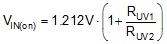
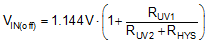
The precision EN input supports adjustable input undervoltage lockout (UVLO) with hysteresis programmed independently through the HYS pin for application specific power-up and power-down requirements. EN connects to a comparator-based input referenced to a 1.212-V bandgap voltage with 68-mV hysteresis. An external logic signal can be used to drive the EN input to toggle the output on and off and for system sequencing or protection. The simplest way to enable the LM5165 operation is to connect EN directly to VIN. This allows the LM5165 to start up when VIN is within its valid operating range. However, many applications benefit from using a resistor divider RUV1 and RUV2 as shown in Figure 7-5 to establish a precision UVLO level. In tandem with the EN setting, use HYS to increase the voltage hysteresis as needed.

Figure 7-5 Programmable Input Voltage UVLO With (a) Fixed Hysteresis, (b) Adjustable Hysteresis

Use Equation 6 and Equation 7 to calculate the input UVLO voltages turnon and turnoff voltages, respectively.

Equation 6. GUID-0C9CD503-4CDE-40DA-BE6E-3C0A8D17063E-low.gif
Equation 7. GUID-91CB2E11-C68C-4CF6-A9EC-48B9890ACE3F-low.gif

There is also a low IQ shutdown mode when EN is pulled below a base-emitter voltage drop (approximately 0.6 V at room temperature). If EN is below this hard shutdown threshold, the internal LDO regulator powers off and the internal bias supply rail collapses, shutting down the bias currents of the LM5165. The LM5165 operates in standby mode when the EN voltage is between the hard shutdown and precision enable thresholds.