SNVSBS7A December 2021 – September 2022 LM5168 , LM5169
PRODUCTION DATA
- 1 Features
- 2 Applications
- 3 Description
- 4 Revision History
- 5 Device Comparison Table
- 6 Pin Configuration and Functions
- 7 Specifications
-
8 Detailed Description
- 8.1 Overview
- 8.2 Functional Block Diagram
- 8.3
Feature Description
- 8.3.1 Control Architecture
- 8.3.2 Internal VCC Regulator and Bootstrap Capacitor
- 8.3.3 Internal Soft Start
- 8.3.4 On-Time Generator
- 8.3.5 Current Limit
- 8.3.6 N-Channel Buck Switch and Driver
- 8.3.7 Synchronous Rectifier
- 8.3.8 Enable, Undervoltage Lockout (EN/UVLO)
- 8.3.9 Power Good (PGOOD)
- 8.3.10 Thermal Protection
- 8.4 Device Functional Modes
-
9 Application and Implementation
- 9.1 Application Information
- 9.2
Typical Fly-Buck™ Converter Application
- 9.2.1 Design Requirements
- 9.2.2
Detailed Design Procedure
- 9.2.2.1 Switching Frequency (RT)
- 9.2.2.2 Transformer Selection
- 9.2.2.3 Output Capacitor Selection
- 9.2.2.4 Secondary Output Diode
- 9.2.2.5 Setting Output Voltage
- 9.2.2.6 Input Capacitor
- 9.2.2.7 Type-3 Ripple Network
- 9.2.2.8 CBST Selection
- 9.2.2.9 Minimum Secondary Output Load
- 9.2.2.10 Example Design Summary
- 9.2.3 Application Curves
- 9.3 Typical Buck Application
- 9.4 Power Supply Recommendations
- 9.5 Layout
- 10Device and Documentation Support
- 11Mechanical, Packaging, and Orderable Information
Package Options
Mechanical Data (Package|Pins)
- DDA|8
Thermal pad, mechanical data (Package|Pins)
- DDA|8
Orderable Information
9.5.1 Thermal Considerations
As with any power conversion device, the LM516x dissipates internal power while operating. The effect of this power dissipation is to raise the internal temperature of the converter above ambient. The internal die temperature (TJ) is a function of the following:
- Ambient temperature
- Power loss
- Effective thermal resistance, RθJA, of the application
- PCB layout
The maximum internal die temperature for the LM516x must be limited to 150°C. This establishes a limit on the maximum device power dissipation and, therefore, the load current. Equation 37 shows the relationships between the important parameters. It is easy to see that larger ambient temperatures (TA) and larger values of RθJA reduce the maximum available output current. The converter efficiency can be estimated by using the curves provided in this data sheet. Note that these curves include the power loss in the inductor. If the desired operating conditions cannot be found in one of the curves, then interpolation can be used to estimate the efficiency. Alternatively, the EVM can be adjusted to match the desired application requirements and the efficiency can be measured directly. The correct value of RθJA is more difficult to estimate. As stated in the Semiconductor and IC Package Thermal Metrics Application Report, the value of RθJA given in the Thermal Information table is not valid for design purposes and must not be used to estimate the thermal performance of the application. The values reported in that table were measured under a specific set of conditions that are rarely obtained in an actual application. The data given for RθJC(bott) and ΨJT can be useful when determining thermal performance. The value of RθJA(EVM) is applicable to the LM5168PEVM and is given for reference only. See the Semiconductor and IC Package Thermal Metrics Application Report for more information and the resources given at the end of this section.
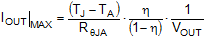
where
- η is the efficiency.
The effective RθJA is a critical parameter and depends on many factors such as the following:
- Power dissipation
- Air temperature, flow
- PCB area
- Copper heat-sink area
- Number of thermal vias under the package
- Adjacent component placement
The LM516x features a die attach paddle, or "thermal pad" (EP), to provide a place to solder down to the PCB heat-sinking copper. This provides a good heat conduction path from the regulator junction to the heat sink and must be properly soldered to the PCB heat sink copper. Typical examples of RΘJA can be found in Figure 9-33. The copper area given in the graph is for each layer. The top and bottom layers are 2-oz copper each, while the inner layers are 1 oz.
The data in Figure 9-34 and Figure 9-35 can be used as a guide to determine the maximum output current for a given set of conditions. The particular conditions under which these graphs were taken are indicated in the notes below each graph.
| VOUT = 5 V | L = 68 μH | FSW = 500 kHz |
| RΘJA = 24 ºC/W |
| VOUT = 12 V | L = 68 μH | FSW = 500 kHz |
| RΘJA = 24 ºC/W |
Remember that the data given in Figure 9-33 through Figure 9-35 is for illustration purposes only, and the actual performance in any given application depends on all of the previously mentioned factors.
The following resources can be used as a guide to optimal thermal PCB design and estimating RθJA for a given application environment:
- Semiconductor and IC Package Thermal Metrics Application Report
- AN-2020 Thermal Design By Insight, Not Hindsight Application Report
- A Guide to Board Layout for Best Thermal Resistance for Exposed Pad Packages Application Report
- Using New Thermal Metrics Application Report
- PCB Thermal Design Tips for Automotive DC/DC Converters Application Report