SNVSBS7A December 2021 – September 2022 LM5168 , LM5169
PRODUCTION DATA
- 1 Features
- 2 Applications
- 3 Description
- 4 Revision History
- 5 Device Comparison Table
- 6 Pin Configuration and Functions
- 7 Specifications
-
8 Detailed Description
- 8.1 Overview
- 8.2 Functional Block Diagram
- 8.3
Feature Description
- 8.3.1 Control Architecture
- 8.3.2 Internal VCC Regulator and Bootstrap Capacitor
- 8.3.3 Internal Soft Start
- 8.3.4 On-Time Generator
- 8.3.5 Current Limit
- 8.3.6 N-Channel Buck Switch and Driver
- 8.3.7 Synchronous Rectifier
- 8.3.8 Enable, Undervoltage Lockout (EN/UVLO)
- 8.3.9 Power Good (PGOOD)
- 8.3.10 Thermal Protection
- 8.4 Device Functional Modes
-
9 Application and Implementation
- 9.1 Application Information
- 9.2
Typical Fly-Buck™ Converter Application
- 9.2.1 Design Requirements
- 9.2.2
Detailed Design Procedure
- 9.2.2.1 Switching Frequency (RT)
- 9.2.2.2 Transformer Selection
- 9.2.2.3 Output Capacitor Selection
- 9.2.2.4 Secondary Output Diode
- 9.2.2.5 Setting Output Voltage
- 9.2.2.6 Input Capacitor
- 9.2.2.7 Type-3 Ripple Network
- 9.2.2.8 CBST Selection
- 9.2.2.9 Minimum Secondary Output Load
- 9.2.2.10 Example Design Summary
- 9.2.3 Application Curves
- 9.3 Typical Buck Application
- 9.4 Power Supply Recommendations
- 9.5 Layout
- 10Device and Documentation Support
- 11Mechanical, Packaging, and Orderable Information
Package Options
Mechanical Data (Package|Pins)
- DDA|8
Thermal pad, mechanical data (Package|Pins)
- DDA|8
Orderable Information
9.3.2.1 Switching Frequency (RT)
The switching frequency of the LM5168 is set by the on-time programming resistor connected to the RT pin. Equation 23 is used to calculate RT based on the desired switching frequency and output voltage. For this example of 500 kHz and 5 V, 24.9 kΩ is used.
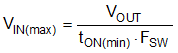
Note that at very low duty cycles, the 50-ns minimum controllable on time of the high-side MOSFET, tON(min), limits the maximum switching frequency. In CCM, tON(min) limits the voltage conversion step-down ratio for a given switching frequency. Use Equation 24 to calculate the minimum controllable duty cycle.

Ultimately, the choice of switching frequency for a given output voltage affects the available input voltage range, solution size, and efficiency. Use Equation 25 to calculate the maximum supply voltage for a given tON(min) to maintain the full switching frequency.