SNVSBJ0B December 2019 – August 2021 LM5170
PRODUCTION DATA
- 1 Features
- 2 Applications
- 3 Description
- 4 Revision History
- 5 Description (continued)
- 6 Pin Configuration and Functions
- 7 Specifications
-
8 Detailed Description
- 8.1 Overview
- 8.2 Functional Block Diagram
- 8.3
Feature Description
- 8.3.1 Bias Supply (VCC, VCCA)
- 8.3.2 Undervoltage Lockout (UVLO) and Master Enable or Disable
- 8.3.3 High Voltage Input (VIN, VINX)
- 8.3.4 Current Sense Amplifier
- 8.3.5 Control Commands
- 8.3.6 Channel Current Monitor (IOUT1, IOUT2)
- 8.3.7 Cycle-by-Cycle Peak Current Limit (IPK)
- 8.3.8 Error Amplifier
- 8.3.9 Ramp Generator
- 8.3.10 Soft Start
- 8.3.11 Gate Drive Outputs, Dead Time Programming, and Adaptive Dead Time (HO1, HO2, LO1, LO2, DT)
- 8.3.12 PWM Comparator
- 8.3.13 Oscillator (OSC)
- 8.3.14 Synchronization to an External Clock (SYNCIN, SYNCOUT)
- 8.3.15 Diode Emulation
- 8.3.16 Power MOSFET Failure Detection and Failure Protection (nFAULT, BRKG, BRKS)
- 8.3.17 Overvoltage Protection (OVPA, OVPB)
- 8.4 Device Functional Modes
- 8.5 Programming
-
9 Application and Implementation
- 9.1 Application Information
- 9.2
Typical Application
- 9.2.1
60-A, Dual-Phase, 48-V to 12-V Bidirectional Converter
- 9.2.1.1 Design Requirements
- 9.2.1.2
Detailed Design Procedure
- 9.2.1.2.1 Determining the Duty Cycle
- 9.2.1.2.2 Oscillator Programming
- 9.2.1.2.3 Power Inductor, RMS and Peak Currents
- 9.2.1.2.4 Current Sense (RCS)
- 9.2.1.2.5 Current Setting Limits (ISETA or ISETD)
- 9.2.1.2.6 Peak Current Limit
- 9.2.1.2.7 Power MOSFETS
- 9.2.1.2.8 Bias Supply
- 9.2.1.2.9 Bootstrap
- 9.2.1.2.10 RAMP Generators
- 9.2.1.2.11 OVP
- 9.2.1.2.12 Dead Time
- 9.2.1.2.13 IOUT Monitors
- 9.2.1.2.14 UVLO Pin Usage
- 9.2.1.2.15 VIN Pin Configuration
- 9.2.1.2.16 Loop Compensation
- 9.2.1.2.17 Soft Start
- 9.2.1.2.18 ISET Pins
- 9.2.1.3 Application Curves
- 9.2.1
60-A, Dual-Phase, 48-V to 12-V Bidirectional Converter
- 10Power Supply Recommendations
- 11Layout
- 12Device and Documentation Support
- 13Mechanical, Packaging, and Orderable Information
Package Options
Mechanical Data (Package|Pins)
- PHP|48
Thermal pad, mechanical data (Package|Pins)
- PHP|48
Orderable Information
8.3.9 Ramp Generator
Refer to Figure 8-7 for the following:
- Circuit block diagram for the ramp generator
- gm error amplifier
- PWM comparator
- Soft-start control circuit
 Figure 8-7 Error Amplifier, Ramp Generator, Soft Start, and PWM Comparator
When the LM5170 is enabled, CRAMP1/2 is charged by the VINX pin through RRAMP1/2 at the beginning of each switching cycle. The internal pulldown FET discharges CRAMP1/2 at the end of the cycle within a 200-ns internal. Then the pulldown is released, and CRAMP1/2 repeats the charging and discharging cycles. In general, the RAMP RC time constant is much greater than the period of a switching cycle. Therefore, the RAMP pin voltages are sawtooth signals with a slope proportional to the HV-Port voltage. This way, the RAMP signals convey the line voltage info. Being directly used by the PWM comparators to determine the instantaneous switching duty cycles, the RAMP signals fulfill the line voltage feedforward function and enable the LM5170 to have a fast response to line transients.
TI recommends you to select appropriate RRAMP and CRAMP values by the following equation such that the RAMP pins reach the peak value of approximately 5 V each cycle when VIN is at 48 V.
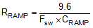
For instance, if Fsw = 100 kHz and CRAMP1 = CRAMP2 = 1 nF, a resistor of approximately 96 kΩ must be selected for RRAMP1 and RRAMP2.
Because CRAMP1/2 must be fully discharged every cycle through the 15-Ω channel resistor of the pulldown FET within the 150-ns minimum discharging interval, CRAMP1/2 must be limited to be less than 2.5 nF nominal at room temperature.
There is also a valid RAMP signal detection circuit for each channel to prevent the channel from errantly running into the maximum duty cycle if RAMP goes away. It detects the peak voltage of the RAMP signal. If the peak voltage is less than 0.6 V in consecutive cycles, it is considered an invalid RAMP and the channel stops switching by turning both HO and LO off until the RAMP signal recovers. This 0.6-V voltage threshold defines the minimum operating voltage of the HV-Port to be approximately 5.76 V.