SNVSBJ0B December 2019 – August 2021 LM5170
PRODUCTION DATA
- 1 Features
- 2 Applications
- 3 Description
- 4 Revision History
- 5 Description (continued)
- 6 Pin Configuration and Functions
- 7 Specifications
-
8 Detailed Description
- 8.1 Overview
- 8.2 Functional Block Diagram
- 8.3
Feature Description
- 8.3.1 Bias Supply (VCC, VCCA)
- 8.3.2 Undervoltage Lockout (UVLO) and Master Enable or Disable
- 8.3.3 High Voltage Input (VIN, VINX)
- 8.3.4 Current Sense Amplifier
- 8.3.5 Control Commands
- 8.3.6 Channel Current Monitor (IOUT1, IOUT2)
- 8.3.7 Cycle-by-Cycle Peak Current Limit (IPK)
- 8.3.8 Error Amplifier
- 8.3.9 Ramp Generator
- 8.3.10 Soft Start
- 8.3.11 Gate Drive Outputs, Dead Time Programming, and Adaptive Dead Time (HO1, HO2, LO1, LO2, DT)
- 8.3.12 PWM Comparator
- 8.3.13 Oscillator (OSC)
- 8.3.14 Synchronization to an External Clock (SYNCIN, SYNCOUT)
- 8.3.15 Diode Emulation
- 8.3.16 Power MOSFET Failure Detection and Failure Protection (nFAULT, BRKG, BRKS)
- 8.3.17 Overvoltage Protection (OVPA, OVPB)
- 8.4 Device Functional Modes
- 8.5 Programming
-
9 Application and Implementation
- 9.1 Application Information
- 9.2
Typical Application
- 9.2.1
60-A, Dual-Phase, 48-V to 12-V Bidirectional Converter
- 9.2.1.1 Design Requirements
- 9.2.1.2
Detailed Design Procedure
- 9.2.1.2.1 Determining the Duty Cycle
- 9.2.1.2.2 Oscillator Programming
- 9.2.1.2.3 Power Inductor, RMS and Peak Currents
- 9.2.1.2.4 Current Sense (RCS)
- 9.2.1.2.5 Current Setting Limits (ISETA or ISETD)
- 9.2.1.2.6 Peak Current Limit
- 9.2.1.2.7 Power MOSFETS
- 9.2.1.2.8 Bias Supply
- 9.2.1.2.9 Bootstrap
- 9.2.1.2.10 RAMP Generators
- 9.2.1.2.11 OVP
- 9.2.1.2.12 Dead Time
- 9.2.1.2.13 IOUT Monitors
- 9.2.1.2.14 UVLO Pin Usage
- 9.2.1.2.15 VIN Pin Configuration
- 9.2.1.2.16 Loop Compensation
- 9.2.1.2.17 Soft Start
- 9.2.1.2.18 ISET Pins
- 9.2.1.3 Application Curves
- 9.2.1
60-A, Dual-Phase, 48-V to 12-V Bidirectional Converter
- 10Power Supply Recommendations
- 11Layout
- 12Device and Documentation Support
- 13Mechanical, Packaging, and Orderable Information
Package Options
Mechanical Data (Package|Pins)
- PHP|48
Thermal pad, mechanical data (Package|Pins)
- PHP|48
Orderable Information
9.1.2.2 Inner Current Loop Compensation
Equation 24 indicates that the power plant is basically a first-order system. A Type-II compensator as shown in Figure 9-3 is adequate to stabilize the loop for both buck and boost mode operations.
Assuming the output impedance of the gm amplifier is RGM, the gain from the inductor to the output of gm amplifier is determined by Equation 25:
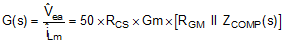
where
- the coefficient 50 is the current sense amplifier gain
- Gm is the transconductance of the gm error amplifier, which is 1 mA/V
- ZCOMP(s) is the equivalent impedance of the compensation network seen at the COMP pin (see Equation 26)
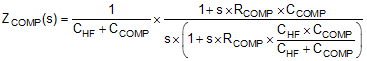
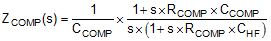
Usually CHF is << CCOMP. Thus, Equation 26 can be simplified to Equation 27:
Because RGM is > 5 MegΩ and the frequency range for loop compensation is usually above a few kHz, the effects of RGM on the loop gain in the interested frequency range becomes negligible. Therefore, substituting Equation 28 into Equation 25, and neglecting RGM, you can get the following:
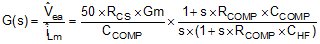
The total open-loop gain of the inner current loop is the product of H(s) and G(s):

Or
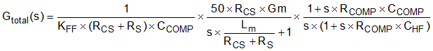
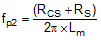
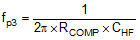
The poles and zeros of the total loop transfer function are determined by:

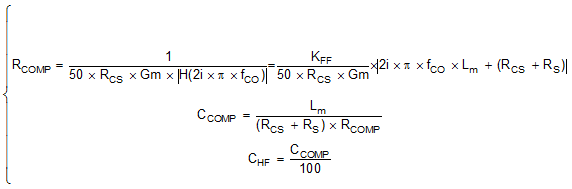
To tailor the total inner current loop gain to cross over at fCO, select the components of the compensation network according to the following guidelines, then fine tune the network for optimal loop performance.
- The zero fz is placed at the power stage pole fp2
- The pole fp3 is placed at approximately two decade higher then fCO
- The total open-loop gain is set to unity at fCO, namely
Therefore, the compensation components can be derived from the above equations, as shown in Equation 36.