SNAS660D June   2015  – May 2021 LM53600-Q1 , LM53601-Q1

PRODUCTION DATA  

  1. Features
  2. Applications
  3. Description
  4. Revision History
  5. Device Comparison
  6. Pin Configuration and Functions
  7. Specifications
    1. 7.1 Absolute Maximum Ratings
    2. 7.2 ESD Ratings
    3. 7.3 Recommended Operating Conditions
    4. 7.4 Thermal Information
    5. 7.5 Electrical Characteristics
    6. 7.6 System Characteristics
    7. 7.7 Timing Requirements
    8. 7.8 Typical Characteristics
  8. Detailed Description
    1. 8.1 Overview
    2. 8.2 Functional Block Diagram
    3. 8.3 Feature Description
      1. 8.3.1 Control Scheme
      2. 8.3.2 Soft-Start Function
      3. 8.3.3 Current Limit
      4. 8.3.4 Hiccup Mode
      5. 8.3.5 RESET Function
      6. 8.3.6 Forced PWM Operation
      7. 8.3.7 Auto Mode Operation and IQ_VIN
      8. 8.3.8 SYNC Operation
      9. 8.3.9 Spread Spectrum
    4. 8.4 Device Functional Modes
      1. 8.4.1 Shutdown
      2. 8.4.2 FPWM Operation
      3. 8.4.3 Auto Mode Operation
  9. Applications and Implementation
    1. 9.1 Application Information
    2. 9.2 Typical Applications
      1. 9.2.1 Off-Battery 5-V, 1-A Output Automotive Converter with Spread Spectrum
        1. 9.2.1.1 Design Requirements
        2. 9.2.1.2 Detailed Design Procedure
          1. 9.2.1.2.1 Inductor Selection
          2. 9.2.1.2.2 Output Capacitor Selection
          3. 9.2.1.2.3 Input Capacitor Selection
          4. 9.2.1.2.4 FB Voltage Divider for Adjustable Versions
          5. 9.2.1.2.5 RPU - RESET Pull Up Resistor
        3. 9.2.1.3 Application Curves
      2. 9.2.2 Off-Battery 3.3 V, 1 A Output Automotive Converter with Spread Spectrum
        1. 9.2.2.1 Design Requirements
        2. 9.2.2.2 Design Procedure
        3. 9.2.2.3 Application Curves
    3. 9.3 Do's and Don't's
  10. 10Power Supply Recommendations
  11. 11Layout
    1. 11.1 Layout Guidelines
      1. 11.1.1 Ground and Thermal Plane Considerations
    2. 11.2 Layout Example
  12. 12Device and Documentation Support
    1. 12.1 Documentation Support
      1. 12.1.1 Related Documentation
    2. 12.2 Receiving Notification of Documentation Updates
    3. 12.3 Support Resources
    4. 12.4 Trademarks
    5. 12.5 Electrostatic Discharge Caution
    6. 12.6 Glossary
  13. 13Mechanical, Packaging, and Orderable Information

Package Options

Mechanical Data (Package|Pins)
Thermal pad, mechanical data (Package|Pins)
Orderable Information

Application Curves

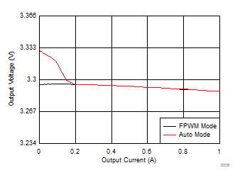
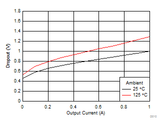
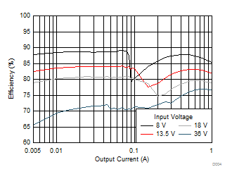
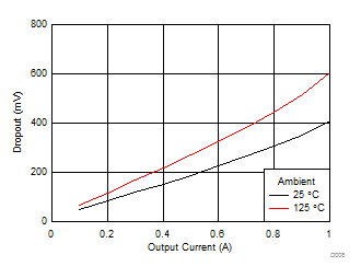
The following characteristics apply only to the circuit shown in Figure 9-12. These parameters are not tested and represent typical performance only. Unless otherwise stated, the following conditions apply: VIN = 13.5 V, TA = 25°C.
The following characteristics apply only to the circuit shown in Figure 9-12. These parameters are not tested and represent typical performance only. Unless otherwise stated, the following conditions apply: VIN = 13.5 V, TA = 25°C.GUID-87E1B486-EDFC-47FF-BC62-D3976B882E77-low.gif
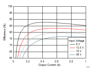
Device Type = 1 A Mode = FPWM 3.3-V Fixed Output
Figure 9-13 Efficiency. The following characteristics apply only to the circuit shown in Figure 9-12. These parameters are not tested and represent typical performance only. Unless otherwise stated, the following conditions apply: VIN = 13.5 V, TA = 25°C.
GUID-7D450AFE-15C5-4759-B6C3-6DCF0DED79BD-low.gif
Device Type = 1 A 3.3-V Fixed Output
Figure 9-15 Load Regulation
GUID-9680CB98-0921-47F2-9BCE-0CD96C062646-low.gif
Device Type = 1 A 3.3-V Fixed Output
92-mΩ Inductor Frequency Drops to 1.85 MHz
Figure 9-17 Entry into Dropout
GUID-CCCD9216-95C8-4DA0-B658-E31B3D3B984B-low.gif
Device Type = 1 A Mode = Auto 3.3-V Fixed Output
Figure 9-14 Efficiency
GUID-1E34A096-9472-4424-B9CE-9D02755DB155-low.gif
Device Type = 1 A Output = 3.2 V 92-mΩ Inductor
3.3-V Fixed Output
Figure 9-16 Dropout Voltage
GUID-2BA60CD5-956F-4964-A901-9D0A981D77F6-low.gif
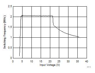
Device Type = 1 A Spread Spectrum
3.3-V Fixed Output Load = 500 mA
Figure 9-18 Frequency vs. Input Voltage