SNAS660D June 2015 – May 2021 LM53600-Q1 , LM53601-Q1
PRODUCTION DATA
- 1 Features
- 2 Applications
- 3 Description
- 4 Revision History
- 5 Device Comparison
- 6 Pin Configuration and Functions
- 7 Specifications
- 8 Detailed Description
- 9 Applications and Implementation
- 10Power Supply Recommendations
- 11Layout
- 12Device and Documentation Support
- 13Mechanical, Packaging, and Orderable Information
Package Options
Mechanical Data (Package|Pins)
- DSX|10
Thermal pad, mechanical data (Package|Pins)
- DSX|10
Orderable Information
9.1 Application Information
The LM53600-Q1 and LM53601-Q1 are step-down DC–DC converters, typically used to convert a higher DC voltage to a lower DC voltage with a maximum output current of either 1 A or 650 mA. The following design procedure can be used to select components for the LM53600-Q1 or LM53601-Q1. Alternately, the WEBENCH® Design Tool may be used to generate a complete design. This tool utilizes an iterative design procedure and has access to a comprehensive database of components. This allows the tool to create an optimized design and allows the user to experiment with various design options.
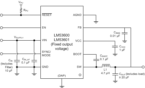
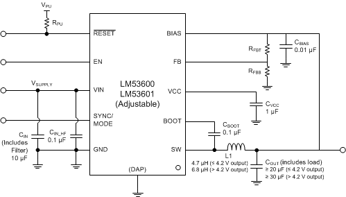
Figure 9-1 shows the minimum required application circuit for the fixed output voltage versions, while Figure 9-2 shows the connections for complete processor control of the LM53601-Q1. Please refer to these figures while following the design procedures. Table 9-2 provides an example of typical design requirements.
 Figure 9-1 Off Battery, Automotive, Fixed Output Voltage, Buck, 2.1 MHz, Spread Spectrum
 Figure 9-2 Off Battery, Automotive, Adjustable Output Voltage, Buck, 2.1 MHz, Spread Spectrum