SNVSAA7B December 2015 – July 2021 LM53625-Q1 , LM53635-Q1
PRODUCTION DATA
- 1 Features
- 2 Applications
- 3 Description
- 4 Revision History
- 5 Device Comparison
- 6 Pin Configuration and Functions
- 7 Specifications
- 8 Detailed Description
-
9 Application and Implementation
- 9.1 Application Information
- 9.2
Typical Applications
- 9.2.1 General Application
- 9.2.2 Fixed 5-V Output for USB-Type Applications
- 9.2.3 Fixed 3.3-V Output
- 9.2.4 Adjustable Output
- 9.3 What to Do and What Not to Do
- 10Power Supply Recommendations
- 11Layout
- 12Device and Documentation Support
- 13Mechanical, Packaging, and Orderable Information
Package Options
Refer to the PDF data sheet for device specific package drawings
Mechanical Data (Package|Pins)
- RNL|22
Thermal pad, mechanical data (Package|Pins)
- RNL|22
Orderable Information
8.4.1 AUTO Mode
In AUTO mode the device moves between PWM and PFM as the load changes. At light loads the regulator operates in PFM . At higher loads the mode changes to PWM. The load currents at which the mode changes can be found in the Section 9.2.2.3.
In PWM, the converter operates as a constant frequency, current mode, full synchronous converter using PWM to regulate the output voltage. While operating in this mode the output voltage is regulated by switching at a constant frequency and modulating the duty cycle to control the power to the load. This provides excellent line and load regulation and low output voltage ripple. When in PWM the converter synchronizes to any valid clock signal on the SYNC input (see Section 8.4.3 and Section 8.4.4 ).
In PFM the high side FET is turned on in a burst of one or more cycles to provide energy to the load. The frequency of these bursts is adjusted to regulate the output, while diode emulation is used to maximize efficiency (see the Glossary). This mode provides high light-load efficiency by reducing the amount of input supply current required to regulate the output voltage at small loads. This trades off very good light load efficiency for larger output voltage ripple and variable switching frequency. Also, a small increase in the output voltage occurs in PFM. The actual switching frequency and output voltage ripple will depend on the input voltage, output voltage, and load. Typical switching waveforms for PFM are shown in Figure 8-8. See the Section 9.2.2.3 for output voltage variation in AUTO mode. The SYNC input is ignored during PFM operation.
A unique feature of this device is that a minimum input voltage is required for the regulator to switch from PWM to PFM at light load. This feature is a consequence of the advanced architecture employed to provide high efficiency at light loads. Figure 8-9 and Figure 8-10 indicates typical values of input voltage required to switch modes at no load. Also, once the regulator switches to PFM, at light load, it remains in that mode if the input voltage is reduced.
 Figure 8-8 Typical PFM Switching Waveforms
 Figure 8-10 Input Voltage for Mode Change — Fixed 3.3-V Output, 2.2-µH Inductor
 Figure 8-9 Input Voltage for Mode Change — Fixed 5-V Output, 2.2-µH Inductor
IQ_VIN is the current consumed by a converter utilizing a LM53635-Q1 or LM53625-Q1 device while regulating without a load. While operating without a load, the LM53635-Q1 or LM53625-Q1 is only powering itself. The device draws power from two sources, its VIN pin, IQ, and either its FB pin for fixed versions or BIAS pin for adjustable versions, IB. Since BIAS or FB is connected to the output of the circuit, the power consumed is converted from input power with an effective efficiency, ηeff, of approximately 80 %. Here, effective efficiency is the added input power needed when lightly loading the converter of the LM53625-Q1 and LM53635- Q1 devices and is divided by the corresponding additional load. This allows unloaded current to be calculated as follows:
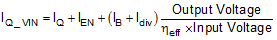
where
- IQ_VIN is the current consumed by the operating (switching) buck converter utilizing the LM53625-Q1 or LM53635-Q1 while unloaded.
- IQ is the current drawn by the LM53625-Q1 or LM53635-Q1 from its VIN terminal. See IQ in Section 7.5.
- IEN is current drawn by the LM53625-Q1 or LM53635-Q1 from its EN terminal. Include this current if EN is connected to VIN. See IEN in Section 7.5. Note that this current drops to a very low value if connected to a voltage less than 5 V.
- IB is bias/feedback current drawn by the LM53625-Q1 or LM53635-Q1 while the Buck converter utilizing it is unloaded. See IB in Section 7.5.
- Idiv is the current drawn by the feedback voltage divider used to set output voltage for adjustable devices. This current is zero for fixed output voltage devices.
- ηeff is the light load efficiency of the Buck converter with IQ_VIN removed from the input current of the buck converter input current. 0.8 is a conservative value that can be used under normal operating conditions.
The EN pin consumes a few micro-amperes when tied to high; see IEN. Add IEN to IQ as shown in Equation 2 if EN is tied to VIN. If EN is tied to a voltage less than 5 V, virtually no current is consumed allowing EN to be used as an UVLO pin once a voltage divider is added.