SNVSAA7B December 2015 – July 2021 LM53625-Q1 , LM53635-Q1
PRODUCTION DATA
- 1 Features
- 2 Applications
- 3 Description
- 4 Revision History
- 5 Device Comparison
- 6 Pin Configuration and Functions
- 7 Specifications
- 8 Detailed Description
-
9 Application and Implementation
- 9.1 Application Information
- 9.2
Typical Applications
- 9.2.1 General Application
- 9.2.2 Fixed 5-V Output for USB-Type Applications
- 9.2.3 Fixed 3.3-V Output
- 9.2.4 Adjustable Output
- 9.3 What to Do and What Not to Do
- 10Power Supply Recommendations
- 11Layout
- 12Device and Documentation Support
- 13Mechanical, Packaging, and Orderable Information
Package Options
Refer to the PDF data sheet for device specific package drawings
Mechanical Data (Package|Pins)
- RNL|22
Thermal pad, mechanical data (Package|Pins)
- RNL|22
Orderable Information
8.1 Overview
The LM53625/35-Q1 is a wide input voltage range, low quiescent current, high performance regulator with internal compensation designed specifically for the automotive market. This device is designed to minimize end-product cost and size while operating in demanding automotive environments. Normal operating frequency is 2.1 MHz allowing the use of small passive components. Because the operating frequency is above the AM band, significant saving in input filtering is also achieved. This device has a low unloaded current consumption eliminating the need for an external back-up LDO. The LM53625/35-Q1 low shutdown current and high maximum operating voltage also allows the elimination of an external load switch. To further reduce system cost, an advanced reset output is provided, which can often eliminate the use of an external reset device.
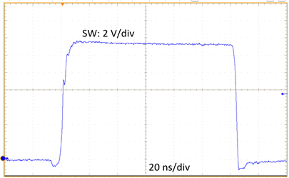
The LM53625/35-Q1 is designed with a flip-chip or HotRod technology, greatly reducing the parasitic inductance of pins. In addition, the layout of the device allows for reduction in the radiated noise generated by the switching action through partial cancellation of the current generated magnetic field.
As a result the switch-node waveform exhibits less overshoot and ringing.
 Figure 8-1 Switch Node Waveform (VIN=13.5V, IOUT=3.5A)
The LM53625/35-Q1 is AEC-Q1 qualified as well as having electrical characteristics ensured up to a maximum junction temperature of 150°C.
The LM53625/35-Q1 is available in VQFN package with wettable-flanks which allows easy inspection of the soldering job without the requirement of X-ray checks.
Please note that, throughout this data sheet, references to the LM53625 apply equally to the LM53635. The difference between the two devices is the maximum output current and specified MOSFET current limits.