SNVSAA7B December   2015  – July 2021 LM53625-Q1 , LM53635-Q1

PRODUCTION DATA  

  1. Features
  2. Applications
  3. Description
  4. Revision History
  5. Device Comparison
  6. Pin Configuration and Functions
  7. Specifications
    1. 7.1 Absolute Maximum Ratings
    2. 7.2 ESD Ratings
    3. 7.3 Recommended Operating Conditions
    4. 7.4 Thermal Information
    5. 7.5 Electrical Characteristics
    6. 7.6 System Characteristics
    7. 7.7 Timing Characteristics
    8. 7.8 Typical Characteristics
  8. Detailed Description
    1. 8.1 Overview
    2. 8.2 Functional Block Diagram
      1. 8.2.1 Control Scheme
    3. 8.3 Feature Description
      1. 8.3.1 RESET Flag Output
      2. 8.3.2 Enable and Start-Up
      3. 8.3.3 Soft-Start Function
      4. 8.3.4 Current Limit
      5. 8.3.5 Hiccup Mode
      6. 8.3.6 Synchronizing Input
      7. 8.3.7 Undervoltage Lockout (UVLO) and Thermal Shutdown (TSD)
      8. 8.3.8 Input Supply Current
    4. 8.4 Device Functional Modes
      1. 8.4.1 AUTO Mode
      2. 8.4.2 FPWM Mode
      3. 8.4.3 Dropout
      4. 8.4.4 Input Voltage Frequency Foldback
    5. 8.5 Spread-Spectrum Operation
  9. Application and Implementation
    1. 9.1 Application Information
    2. 9.2 Typical Applications
      1. 9.2.1 General Application
        1. 9.2.1.1 Design Requirements
        2. 9.2.1.2 Detailed Design Procedure
          1. 9.2.1.2.1 External Components Selection
            1. 9.2.1.2.1.1 Input Capacitors
              1. 9.2.1.2.1.1.1 Input Capacitor Selection
            2. 9.2.1.2.1.2 Output Inductors and Capacitors Selection
              1. 9.2.1.2.1.2.1 Inductor Selection
              2. 9.2.1.2.1.2.2 Output Capacitor Selection
          2. 9.2.1.2.2 Setting the Output Voltage
            1. 9.2.1.2.2.1 FB for Adjustable Versions
          3. 9.2.1.2.3 VCC
          4. 9.2.1.2.4 BIAS
          5. 9.2.1.2.5 CBOOT
          6. 9.2.1.2.6 Maximum Ambient Temperature
        3. 9.2.1.3 Application Curves
      2. 9.2.2 Fixed 5-V Output for USB-Type Applications
        1. 9.2.2.1 Design Requirements
        2. 9.2.2.2 Detailed Design Procedure
        3. 9.2.2.3 Application Curves
      3. 9.2.3 Fixed 3.3-V Output
        1. 9.2.3.1 Design Requirements
        2. 9.2.3.2 Detailed Design Procedure
        3. 9.2.3.3 Application Curves
      4. 9.2.4 Adjustable Output
        1. 9.2.4.1 Design Requirements
        2. 9.2.4.2 Detailed Design Procedure
        3. 9.2.4.3 Application Curves
    3. 9.3 What to Do and What Not to Do
  10. 10Power Supply Recommendations
  11. 11Layout
    1. 11.1 Layout Guidelines
    2. 11.2 Layout Example
  12. 12Device and Documentation Support
    1. 12.1 Device Support
      1. 12.1.1 Third-Party Products Disclaimer
    2. 12.2 Documentation Support
      1. 12.2.1 Related Documentation
    3. 12.3 Receiving Notification of Documentation Updates
    4. 12.4 Support Resources
    5. 12.5 Trademarks
    6. 12.6 Electrostatic Discharge Caution
    7. 12.7 Glossary
  13. 13Mechanical, Packaging, and Orderable Information

Package Options

Refer to the PDF data sheet for device specific package drawings

Mechanical Data (Package|Pins)
  • RNL|22
Thermal pad, mechanical data (Package|Pins)
Orderable Information
FB for Adjustable Versions

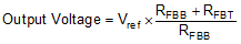
The adjustable version of the LM53625-Q1 and LM53635-Q1 devices regulates output voltage to a level that results in the FB node being VREF, which is approximately 1 V; see Section 7.5. Output voltage given a specific feedback divider can be calculated using Equation 3:

Equation 3. GUID-76C0B4B6-43F8-457F-9338-2D3A0B5E2678-low.gif

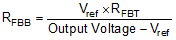
See Figure 9-34 for an example of the use of adjustable versions of the LM53625-Q1 and LM53635-Q1 devices. To ensure proper behavior for all modes of operation, a 50 kΩ resistor is recommended for RFBT. RFBB can then be determined using :

Equation 4. GUID-607EAD19-179F-4F3C-88CA-EAEB2DB2B806-low.gif

In addition a feed-forward capacitor CFF may be required to optimize the transient response. For output voltages greater than 6 V, the WEBENCH Design Tool can be used to optimize the design.