SNVSAA7B December   2015  – July 2021 LM53625-Q1 , LM53635-Q1

PRODUCTION DATA  

  1. Features
  2. Applications
  3. Description
  4. Revision History
  5. Device Comparison
  6. Pin Configuration and Functions
  7. Specifications
    1. 7.1 Absolute Maximum Ratings
    2. 7.2 ESD Ratings
    3. 7.3 Recommended Operating Conditions
    4. 7.4 Thermal Information
    5. 7.5 Electrical Characteristics
    6. 7.6 System Characteristics
    7. 7.7 Timing Characteristics
    8. 7.8 Typical Characteristics
  8. Detailed Description
    1. 8.1 Overview
    2. 8.2 Functional Block Diagram
      1. 8.2.1 Control Scheme
    3. 8.3 Feature Description
      1. 8.3.1 RESET Flag Output
      2. 8.3.2 Enable and Start-Up
      3. 8.3.3 Soft-Start Function
      4. 8.3.4 Current Limit
      5. 8.3.5 Hiccup Mode
      6. 8.3.6 Synchronizing Input
      7. 8.3.7 Undervoltage Lockout (UVLO) and Thermal Shutdown (TSD)
      8. 8.3.8 Input Supply Current
    4. 8.4 Device Functional Modes
      1. 8.4.1 AUTO Mode
      2. 8.4.2 FPWM Mode
      3. 8.4.3 Dropout
      4. 8.4.4 Input Voltage Frequency Foldback
    5. 8.5 Spread-Spectrum Operation
  9. Application and Implementation
    1. 9.1 Application Information
    2. 9.2 Typical Applications
      1. 9.2.1 General Application
        1. 9.2.1.1 Design Requirements
        2. 9.2.1.2 Detailed Design Procedure
          1. 9.2.1.2.1 External Components Selection
            1. 9.2.1.2.1.1 Input Capacitors
              1. 9.2.1.2.1.1.1 Input Capacitor Selection
            2. 9.2.1.2.1.2 Output Inductors and Capacitors Selection
              1. 9.2.1.2.1.2.1 Inductor Selection
              2. 9.2.1.2.1.2.2 Output Capacitor Selection
          2. 9.2.1.2.2 Setting the Output Voltage
            1. 9.2.1.2.2.1 FB for Adjustable Versions
          3. 9.2.1.2.3 VCC
          4. 9.2.1.2.4 BIAS
          5. 9.2.1.2.5 CBOOT
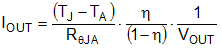
          6. 9.2.1.2.6 Maximum Ambient Temperature
        3. 9.2.1.3 Application Curves
      2. 9.2.2 Fixed 5-V Output for USB-Type Applications
        1. 9.2.2.1 Design Requirements
        2. 9.2.2.2 Detailed Design Procedure
        3. 9.2.2.3 Application Curves
      3. 9.2.3 Fixed 3.3-V Output
        1. 9.2.3.1 Design Requirements
        2. 9.2.3.2 Detailed Design Procedure
        3. 9.2.3.3 Application Curves
      4. 9.2.4 Adjustable Output
        1. 9.2.4.1 Design Requirements
        2. 9.2.4.2 Detailed Design Procedure
        3. 9.2.4.3 Application Curves
    3. 9.3 What to Do and What Not to Do
  10. 10Power Supply Recommendations
  11. 11Layout
    1. 11.1 Layout Guidelines
    2. 11.2 Layout Example
  12. 12Device and Documentation Support
    1. 12.1 Device Support
      1. 12.1.1 Third-Party Products Disclaimer
    2. 12.2 Documentation Support
      1. 12.2.1 Related Documentation
    3. 12.3 Receiving Notification of Documentation Updates
    4. 12.4 Support Resources
    5. 12.5 Trademarks
    6. 12.6 Electrostatic Discharge Caution
    7. 12.7 Glossary
  13. 13Mechanical, Packaging, and Orderable Information

Package Options

Refer to the PDF data sheet for device specific package drawings

Mechanical Data (Package|Pins)
  • RNL|22
Thermal pad, mechanical data (Package|Pins)
Orderable Information
Maximum Ambient Temperature

As with any power conversion device, the LM53625/35-Q1 dissipates internal power while operating. The effect of this power dissipation is to raise the internal temperature of the converter above ambient. The internal die temperature (TJ) is a function of the ambient temperature, the power loss, and the effective thermal resistance, RθJA of the device and PCB combination. The maximum internal die temperature for the LM53625/35-Q1 is 150°C, thus establishing a limit on the maximum device power dissipation and therefore load current at high ambient temperatures. Equation 5 shows the relationships between the important parameters.

Equation 5. GUID-7BF1CE84-B2F3-4507-9565-0E72B90747BE-low.gif

The device uses an advanced package technology that utilizes the pads/pins as heat spreading paths. As a result, the pads should be connected to large copper areas in order to dissipate the heat from the IC. All pins provide some heat relief capability but the PVINs, PGNDs and SW pins are of particular importance for proper heat dissipation. Utilization of all the board layers for heat dissipation using vias as heat pipes is recommended. The Layout Guideline section includes example that shows layout for proper heat management.