SNOSB22C October 2008 – October 2014 LM5574-Q1
PRODUCTION DATA.
- 1 Features
- 2 Applications
- 3 Description
- 4 Revision History
- 5 Pin Configuration and Functions
- 6 Specifications
- 7 Detailed Description
- 8 Application and Implementation
- 9 Power Supply Recommendations
- 10Layout
- 11Device and Documentation Support
- 12Mechanical, Packaging, and Orderable Information
Package Options
Mechanical Data (Package|Pins)
- PW|16
Thermal pad, mechanical data (Package|Pins)
Orderable Information
8 Application and Implementation
NOTE
Information in the following applications sections is not part of the TI component specification, and TI does not warrant its accuracy or completeness. TI’s customers are responsible for determining suitability of components for their purposes. Customers should validate and test their design implementation to confirm system functionality.
8.1 Application Information
8.1.1 Bias Power Dissipation Reduction
Buck regulators operating with high input voltage can dissipate an appreciable amount of power for the bias of the IC. The VCC regulator must step-down the input voltage VIN to a nominal VCC level of 7 V. The large voltage drop across the VCC regulator translates into a large power dissipation within the VCC regulator. There are several techniques that can significantly reduce this bias regulator power dissipation. Figure 14 and Figure 15 depict two methods to bias the IC from the output voltage. In each case the internal VCC regulator is used to initially bias the VCC pin. After the output voltage is established, the VCC pin potential is raised above the nominal 7V regulation level, which effectively disables the internal VCC regulator. The voltage applied to the VCC pin should never exceed 14 V. The VCC voltage should never be larger than the VIN voltage.
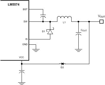 Figure 14. VCC Bias from VOUT for 8 V < VOUT < 14 V
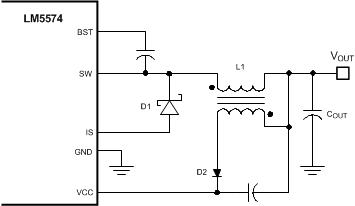 Figure 15. VCC Bias with Additional Winding on the Output Inductor
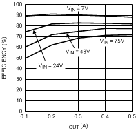
8.2 Typical Application
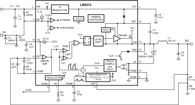 Figure 16. Typical Application Schematic
8.2.1 Design Requirements
The circuit shown in Figure 16 is configured for the following specifications:
- VOUT = 5 V
- VIN = 7 V to 75 V
- Fs = 300 kHz
- Minimum load current (for CCM) = 100 mA
- Maximum load current = 0.5 A
8.2.2 Detailed Design Procedure
8.2.2.1 External Components
The procedure for calculating the external components is illustrated with the following design example.
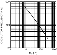
8.2.2.2 R3 (RT)
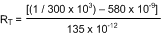
RT sets the oscillator switching frequency. Generally, higher frequency applications are smaller but have higher losses. Operation at 300 kHz was selected for this example as a reasonable compromise for both small size and high efficiency. The value of RT for 300 kHz switching frequency can be calculated as follows:
The nearest standard value of 21 kΩ was chosen for RT.
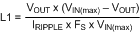
8.2.2.3 L1
The inductor value is determined based on the operating frequency, load current, ripple current, and the minimum and maximum input voltage (VIN(min), VIN(max)).
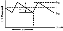 Figure 17. Inductor Current Waveform
To keep the circuit in continuous conduction mode (CCM), the maximum ripple current IRIPPLE should be less than twice the minimum load current, or 0.2 Ap-p. Using this value of ripple current, the value of inductor (L1) is calculated using the following:
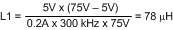
This procedure provides a guide to select the value of L1. The nearest standard value (100 µH) will be used. L1 must be rated for the peak current (IPK+) to prevent saturation. During normal loading conditions, the peak current occurs at maximum load current plus maximum ripple. During an overload condition the peak current is limited to 0.7 A nominal (0.85 A maximum). The selected inductor has a conservative 1.0 Amp saturation current rating. For this manufacturer, the saturation rating is defined as the current necessary for the inductance to reduce by 30%, at 20°C.
8.2.2.4 C3 (CRAMP)
With the inductor value selected, the value of C3 (CRAMP) necessary for the emulation ramp circuit is:
where
- L is in Henrys.
With L1 selected for 100µH the recommended value for C3 is 470 pF (nearest standard value).
8.2.2.5 C9
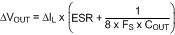
The output capacitor, C9 smoothes the inductor ripple current and provides a source of charge for transient loading conditions. For this design a 22-µF ceramic capacitor was selected. The ceramic capacitor provides ultra low ESR to reduce the output ripple voltage and noise spikes. An approximation for the output ripple voltage is:
8.2.2.6 D1
A Schottky type re-circulating diode is required for all LM5574-Q1 applications. Ultra-fast diodes are not recommended and may result in damage to the IC due to reverse recovery current transients. The near ideal reverse recovery characteristics and low forward voltage drop are particularly important diode characteristics for high input voltage and low output voltage applications common to the LM5574-Q1. The reverse recovery characteristic determines how long the current surge lasts each cycle when the buck switch is turned on. The reverse recovery characteristics of Schottky diodes minimize the peak instantaneous power in the buck switch occurring during turn-on each cycle. The resulting switching losses of the buck switch are significantly reduced when using a Schottky diode. The reverse breakdown rating should be selected for the maximum VIN, plus some safety margin.
The forward voltage drop has a significant impact on the conversion efficiency, especially for applications with a low output voltage. “Rated” current for diodes vary widely from various manufacturers. The worst case is to assume a short circuit load condition. In this case the diode will carry the output current almost continuously. For the LM5574-Q1 this current can be as high as 0.7 A. Assuming a worst case 1 V drop across the diode, the maximum diode power dissipation can be as high as 0.7 W. For the reference design a 100 V Schottky in a SMA package was selected.
8.2.2.7 C1
The regulator supply voltage has a large source impedance at the switching frequency. Good quality input capacitors are necessary to limit the ripple voltage at the VIN pin while supplying most of the switch current during the on-time. When the buck switch turns on, the current into the VIN pin steps to the lower peak of the inductor current waveform, ramps up to the peak value, then drops to zero at turn-off. The average current into VIN during the on-time is the load current. The input capacitance should be selected for RMS current rating and minimum ripple voltage. A good approximation for the required ripple current rating necessary is IRMS > IOUT / 2.
Quality ceramic capacitors with a low ESR should be selected for the input filter. To allow for capacitor tolerances and voltage effects, one 1.0-µF, 100 V ceramic capacitor will be used. If step input voltage transients are expected near the maximum rating of the LM5574-Q1, a careful evaluation of ringing and possible spikes at the device VIN pin should be completed. An additional damping network or input voltage clamp may be required in these cases.
8.2.2.8 C8
The capacitor at the VCC pin provides noise filtering and stability for the VCC regulator. The recommended value of C8 should be no smaller than 0.1-µF, and should be a good quality, low ESR, ceramic capacitor. A value of 0.47-µF was selected for this design.
8.2.2.9 C7
The bootstrap capacitor between the BST and the SW pins supplies the gate current to charge the buck switch gate at turn-on. The recommended value of C7 is 0.022-µF, and should be a good quality, low ESR, ceramic capacitor.
8.2.2.10 C4
The capacitor at the SS pin determines the soft-start time, that is the time for the reference voltage and the output voltage, to reach the final regulated value. The time is determined from:

For this application, a C4 value of 0.01µF was chosen which corresponds to a soft-start time of 1ms.
8.2.2.11 R5, R6
R5 and R6 set the output voltage level, the ratio of these resistors is calculated from:
For a 5V output, the R5/R6 ratio calculates to 3.082. The resistors should be chosen from standard value resistors, a good starting point is selection in the range of 1.0kΩ - 10kΩ. Values of 5.11kΩ for R5, and 1.65kΩ for R6 were selected.
8.2.2.12 R1, R2, C2
A voltage divider can be connected to the SD pin to set a minimum operating voltage VIN(min) for the regulator. If this feature is required, the easiest approach to select the divider resistor values is to select a value for R1 (between 10kΩ and 100kΩ recommended) then calculate R2 from:
Capacitor C2 provides filtering for the divider. The voltage at the SD pin should never exceed 8V, when using an external set-point divider it may be necessary to clamp the SD pin at high input voltage conditions. The reference design utilizes the full range of the LM5574-Q1 (6V to 75V); therefore these components can be omitted. With the SD pin open circuit the LM5574-Q1 responds once the VCC UVLO threshold is satisfied.
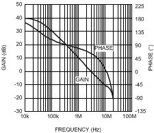
8.2.2.13 R4, C5, C6
These components configure the error amplifier gain characteristics to accomplish a stable overall loop gain. One advantage of current mode control is the ability to close the loop with only two feedback components, R4 and C5. The overall loop gain is the product of the modulator gain and the error amplifier gain. The DC modulator gain of the LM5574-Q1 is as follows:
The dominant low frequency pole of the modulator is determined by the load resistance (RLOAD,) and output capacitance (COUT). The corner frequency of this pole is:
For RLOAD = 20Ω and COUT = 22µF then fp(MOD) = 362Hz
DC Gain(MOD) = 0.5 x 20 = 20dB
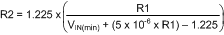
For the design example of Figure 16 the following modulator gain vs. frequency characteristic was measured as shown in Figure 18.
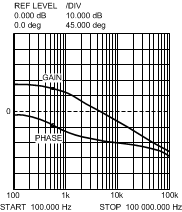
Components R4 and C5 configure the error amplifier as a type II configuration which has a pole at DC and a zero at fZ = 1 / (2πR4C5). The error amplifier zero cancels the modulator pole leaving a single pole response at the crossover frequency of the loop gain. A single pole response at the crossover frequency yields a very stable loop with 90 degrees of phase margin.
For the design example, a target loop bandwidth (crossover frequency) of 25kHz was selected. The compensation network zero (fZ) should be selected at least an order of magnitude less than the target crossover frequency. This constrains the product of R4 and C5 for a desired compensation network zero 1 / (2π R4 C5) to be less than 2kHz. Increasing R4, while proportionally decreasing C5, increases the error amp gain. Conversely, decreasing R4 while proportionally increasing C5, decreases the error amp gain. For the design example C5 was selected for 0.022µF and R4 was selected for 24.9kΩ. These values configure the compensation network zero at 290Hz. The error amp gain at frequencies greater than fZ is: R4 / R5, which is approximately 5 (14dB).
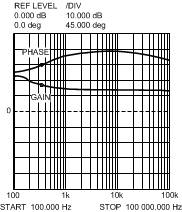 Figure 19. Error Amplifier Gain and Phase
The overall loop can be predicted as the sum (in dB) of the modulator gain and the error amp gain.
 Figure 20. Overall Loop Gain and Phase
If a network analyzer is available, the modulator gain can be measured and the error amplifier gain can be configured for the desired loop transfer function. If a network analyzer is not available, the error amplifier compensation components can be designed with the guidelines given. Step load transient tests can be performed to verify acceptable performance. The step load goal is minimum overshoot with a damped response. C6 can be added to the compensation network to decrease noise susceptibility of the error amplifier. The value of C6 must be sufficiently small since the addition of this capacitor adds a pole in the error amplifier transfer function. This pole must be well beyond the loop crossover frequency. A good approximation of the location of the pole added by C6 is:
8.2.3 Application Curves
AVCL = 101