SNOSB22C October 2008 – October 2014 LM5574-Q1
PRODUCTION DATA.
- 1 Features
- 2 Applications
- 3 Description
- 4 Revision History
- 5 Pin Configuration and Functions
- 6 Specifications
- 7 Detailed Description
- 8 Application and Implementation
- 9 Power Supply Recommendations
- 10Layout
- 11Device and Documentation Support
- 12Mechanical, Packaging, and Orderable Information
Package Options
Mechanical Data (Package|Pins)
- PW|16
Thermal pad, mechanical data (Package|Pins)
Orderable Information
10 Layout
10.1 Layout Guidelines
The circuit in Figure 16 serves as both a block diagram of the LM5575 and a typical application board schematic for the LM5574. In a buck regulator there are two loops where currents are switched very fast. The first loop starts from the input capacitors, to the regulator VIN pin, to the regulator SW pin, to the inductor then out to the load. The second loop starts from the output capacitor ground, to the regulator PGND pins, to the regulator IS pins, to the diode anode, to the inductor and then out to the load. Minimizing the loop area of these two loops reduces the stray inductance and minimizes noise and possible erratic operation. A ground plane in the PC board is recommended as a means to connect the input filter capacitors to the output filter capacitors and the PGND pins of the regulator. Connect all of the low power ground connections (CSS, RT, CRAMP) directly to the regulator AGND pin. Connect the AGND and PGND pins together through the topside copper area covering the entire underside of the device. Place several vias in this underside copper area to the ground plane.
The two highest power dissipating components are the re-circulating diode and the LM5574 regulator IC. The easiest method to determine the power dissipated within the LM5574 is to measure the total conversion losses (PIN – POUT) then subtract the power losses in the Schottky diode, output inductor and snubber resistor. An approximation for the Schottky diode loss is P = (1-D) x Iout x Vfwd. An approximation for the output inductor power is P = IOUT2 x R x 1.1, where R is the DC resistance of the inductor and the 1.1 factor is an approximation for the AC losses. If a snubber is used, an approximation for the damping resistor power dissipation is P = VIN2 x Fsw x Csnub, where Fsw is the switching frequency and Csnub is the snubber capacitor. The regulator has an exposed thermal pad to aid power dissipation. Adding several vias under the device to the ground plane will greatly reduce the regulator junction temperature. Selecting a diode with an exposed pad will aid the power dissipation of the diode.
The most significant variables that affect the power dissipated by the LM5576 are the output current, input voltage and operating frequency. The power dissipated while operating near the maximum output current and maximum input voltage can be appreciable. The operating frequency of the LM5574 evaluation board has been designed for 300 kHz. When operating at 3 A output current with a 70 V input the power dissipation of the LM5574 regulator is approximately 2.5 W.
The junction-to-ambient thermal resistance of the LM5574 will vary with the application. The most significant variables are the area of copper in the PC board, the number of vias under the IC exposed pad and the amount of forced air cooling provided. Referring to the evaluation board artwork, the area under the LM5576 (component side) is covered with copper and there are 5 connection vias to the solder side ground plane. Additional vias under the IC will have diminishing value as more vias are added. The integrity of the solder connection from the IC exposed pad to the PC board is critical. Excessive voids will greatly diminish the thermal dissipation capacity. The junction-to-ambient thermal resistance of the LM5576 mounted in the evaluation board varies from 45°C/W with no airflow to 25°C/W with 900 LFM (Linear Feet per Minute). With a 25°C ambient temperature and no airflow, the predicted junction temperature for the LM5576 will be 25 + (45 x 2.5) = 137.5°C. If the evaluation board is operated at 3 A output current and 70 V input voltage for a prolonged period of time the thermal shutdown protection within the IC will activate. The IC will turn off allowing the junction to cool, followed by restart with the soft-start capacitor reset to zero.
One or more of the following modifications will prevent the thermal shutdown from being activated: apply forced air cooling, reduce the maximum input voltage, lower the maximum output current, reduce the operating frequency, add more heat sinking to the PC board. For example, applying forced air cooling of 225 LFM will reduce the LM5576 thermal resistance to approximately 30°C/W. The junction temperature will be reduced to 25 + (2.5 x 30) = 100°C. If the maximum input voltage for the application is 48 V, then the IC power dissipation reduces to 2 W (at 3 A output current). With the same forced air cooling the junction temperature reduces to 25 + (2 x 30) = 85°C.
10.2 Layout Example
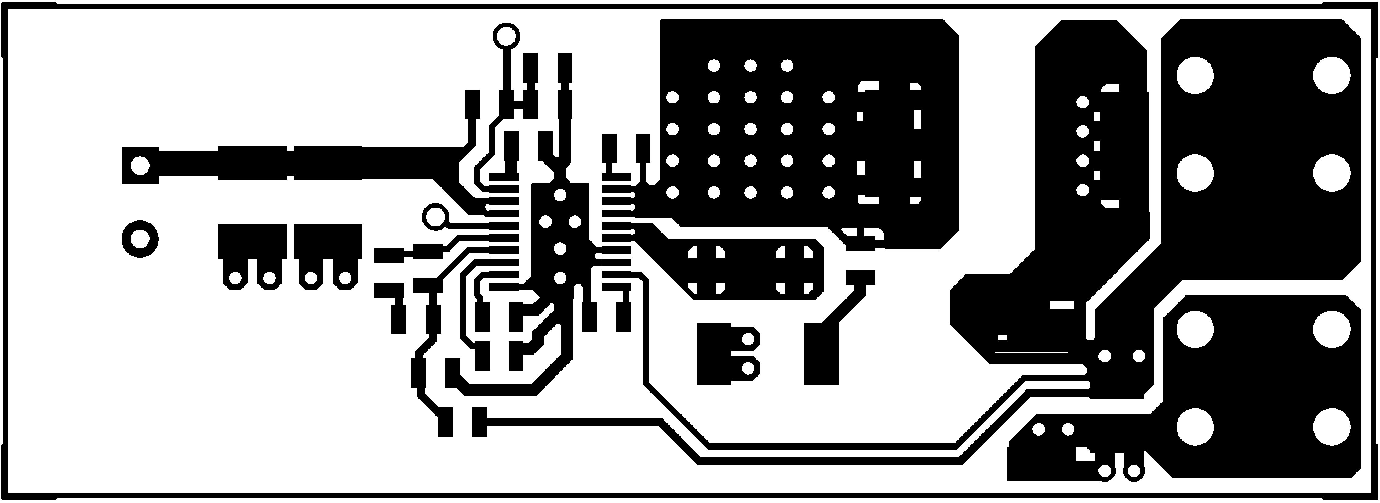 Figure 25. Component Side
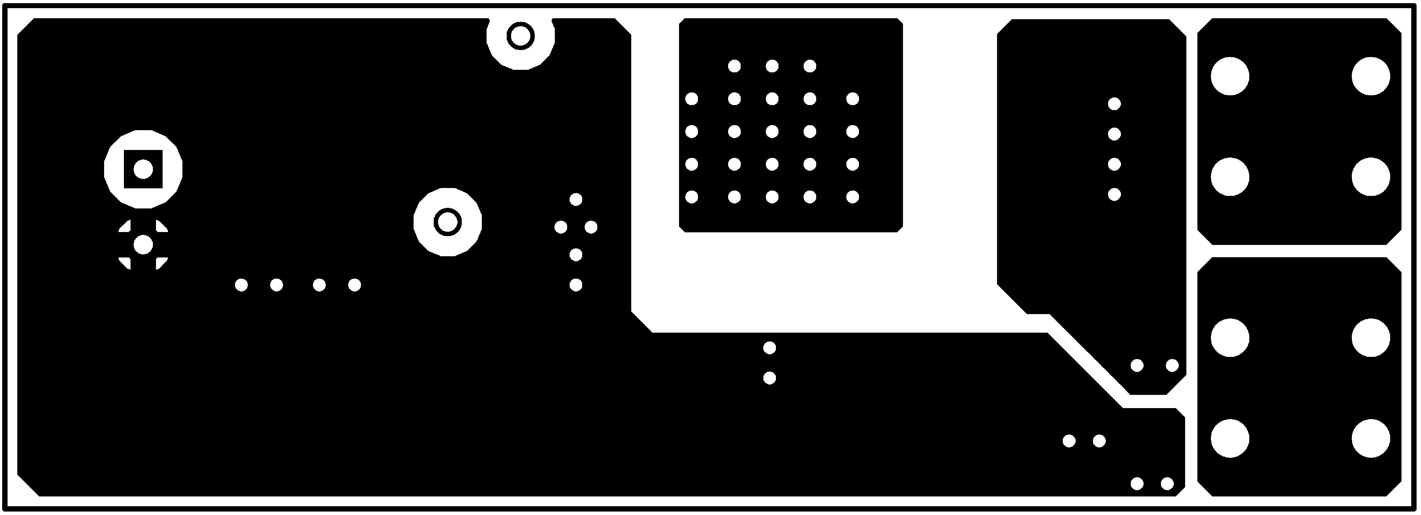 Figure 26. Solder Side
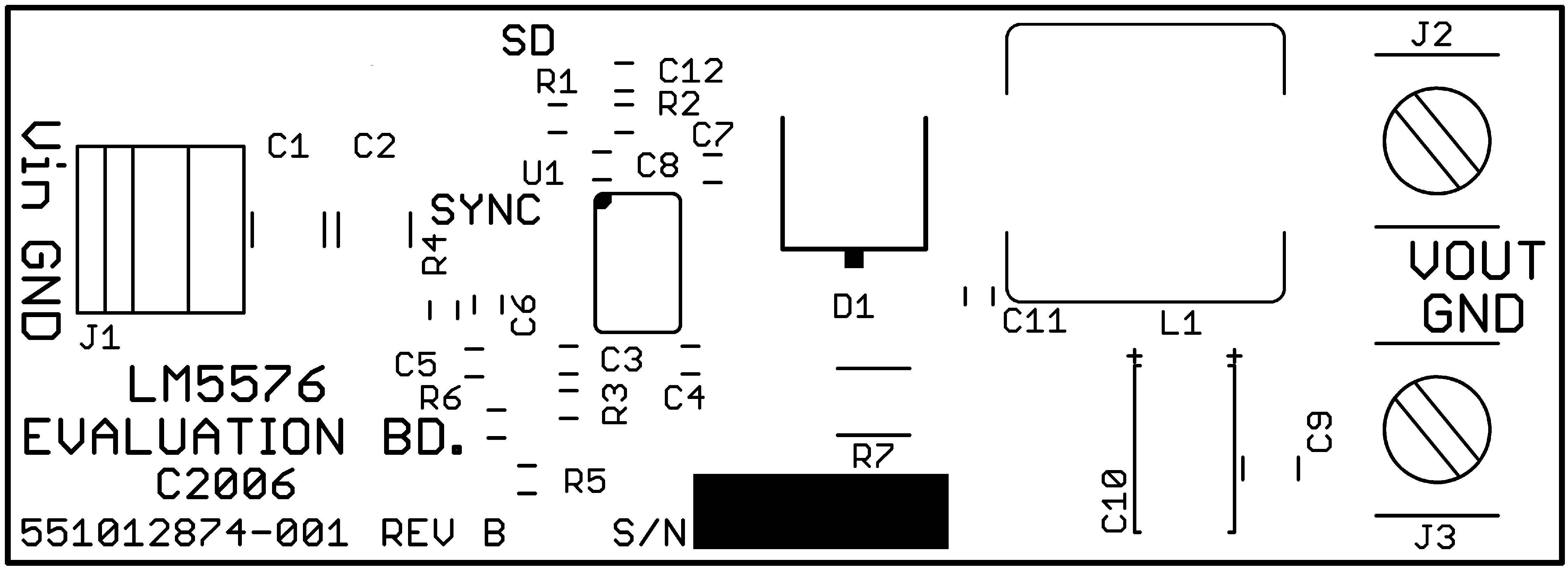 Figure 27. Silkscreen