SNOSB22C October 2008 – October 2014 LM5574-Q1
PRODUCTION DATA.
- 1 Features
- 2 Applications
- 3 Description
- 4 Revision History
- 5 Pin Configuration and Functions
- 6 Specifications
- 7 Detailed Description
- 8 Application and Implementation
- 9 Power Supply Recommendations
- 10Layout
- 11Device and Documentation Support
- 12Mechanical, Packaging, and Orderable Information
Package Options
Mechanical Data (Package|Pins)
- PW|16
Thermal pad, mechanical data (Package|Pins)
Orderable Information
5 Pin Configuration and Functions
16-Pin
TSSOP Package
Top View
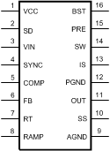
Pin Functions
| PIN | I/O | DESCRIPTION | APPLICATION INFORMATION | |
|---|---|---|---|---|
| NO. | NAME | |||
| 1 | VCC | O | Output of the bias regulator | VCC tracks VIN up to 9 V. Beyond 9 V, VCC is regulated to 7 Volts. A 0.1-uF to 1-uF ceramic decoupling capacitor is required. An external voltage (7.5 V – 14 V) can be applied to this pin to reduce internal power dissipation. |
| 2 | SD | I | Shutdown or UVLO input | If the SD pin voltage is below 0.7 V, the regulator will be in a low power state. If the SD pin voltage is between 0.7 V and 1.225 V, the regulator will be in standby mode. If the SD pin voltage is above 1.225 V the regulator will be operational. An external voltage divider can be used to set a line undervoltage shutdown threshold. If the SD pin is left open circuit, a 5 µA pull-up current source configures the regulator fully operational. |
| 3 | Vin | I | Input supply voltage | Nominal operating range: 6 V to 75 V |
| 4 | SYNC | I | Oscillator synchronization input or output | The internal oscillator can be synchronized to an external clock with an external pull-down device. Multiple LM5574-Q1 devices can be synchronized together by connection of their SYNC pins. |
| 5 | COMP | O | Output of the internal error amplifier | The loop compensation network should be connected between this pin and the FB pin. |
| 6 | FB | I | Feedback signal from the regulated output | This pin is connected to the inverting input of the internal error amplifier. The regulation threshold is 1.225 V. |
| 7 | RT | I | Internal oscillator frequency set input | The internal oscillator is set with a single resistor, connected between this pin and the AGND pin. |
| 8 | RAMP | O | Ramp control signal | An external capacitor connected between this pin and the AGND pin sets the ramp slope used for current mode control. Recommended capacitor range 50 pF to 2000 pF. |
| 9 | AGND | Ground | Analog ground | Internal reference for the regulator control functions |
| 10 | SS | O | Soft-start | An external capacitor and an internal 10 µA current source set the time constant for the rise of the error amp reference. The SS pin is held low during standby, VCC UVLO and thermal shutdown. |
| 11 | OUT | O | Output voltage connection | Connect directly to the regulated output voltage. |
| 12 | PGND | Ground | Power ground | Low side reference for the PRE switch and the IS sense resistor. |
| 13 | IS | I | Current sense | Current measurement connection for the re-circulating diode. An internal sense resistor and a sample/hold circuit sense the diode current near the conclusion of the off-time. This current measurement provides the DC level of the emulated current ramp. |
| 14 | SW | O | Switching node | The source terminal of the internal buck switch. The SW pin should be connected to the external Schottky diode and to the buck inductor. |
| 15 | PRE | O | Pre-charge assist for the bootstrap capacitor | This open drain output can be connected to SW pin to aid charging the bootstrap capacitor during very light load conditions or in applications where the output may be pre-charged before the LM5574-Q1 is enabled. An internal pre-charge MOSFET is turned on for 250 ns each cycle just prior to the on-time interval of the buck switch. |
| 16 | BST | I | Boost input for bootstrap capacitor | An external capacitor is required between the BST and the SW pins. A 0.022-µF ceramic capacitor is recommended. The capacitor is charged from VCC via an internal diode during the off-time of the buck switch. |