SNVSBY6 October 2021 LM61430-Q1
PRODUCTION DATA
- 1 Features
- 2 Applications
- 3 Description
- 4 Revision History
- 5 Device Comparison Table
- 6 Pin Configuration and Functions
- 7 Specifications
-
8 Detailed Description
- 8.1 Overview
- 8.2 Functional Block Diagram
- 8.3
Feature Description
- 8.3.1 EN/SYNC Uses for Enable and VIN UVLO
- 8.3.2 EN/SYNC Pin Uses for Synchronization
- 8.3.3 Clock Locking
- 8.3.4 Adjustable Switching Frequency
- 8.3.5 PGOOD Output Operation
- 8.3.6 Internal LDO, VCC UVLO, and BIAS Input
- 8.3.7 Bootstrap Voltage and VCBOOT-UVLO (CBOOT Pin)
- 8.3.8 Adjustable SW Node Slew Rate
- 8.3.9 Spread Spectrum
- 8.3.10 Soft Start and Recovery From Dropout
- 8.3.11 Output Voltage Setting
- 8.3.12 Overcurrent and Short Circuit Protection
- 8.3.13 Thermal Shutdown
- 8.3.14 Input Supply Current
- 8.4 Device Functional Modes
- 9 Application and Implementation
- 10Power Supply Recommendations
- 11Layout
- 12Device and Documentation Support
- 13Mechanical, Packaging, and Orderable Information
Package Options
Mechanical Data (Package|Pins)
- RJR|14
Thermal pad, mechanical data (Package|Pins)
Orderable Information
10 Power Supply Recommendations
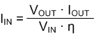
The characteristics of the input supply must be compatible with the Absolute Maximum Ratings and Recommended Operating Conditions in this data sheet. In addition, the input supply must be capable of delivering the required input current to the loaded converter. The average input current can be estimated with Equation 14.
where
- η = efficiency
If the converter is connected to the input supply through long wires or PCB traces, special care is required to achieve good performance. The parasitic inductance and resistance of the input cables can have an adverse effect on the operation of the converter. The parasitic inductance, in combination with the low-ESR, ceramic input capacitors, can form an under-damped resonant circuit, resulting in overvoltage transients at the input to the converter or tripping UVLO. The parasitic resistance can cause the voltage at the VIN pin to dip whenever a load transient is applied to the output. If the application is operating close to the minimum input voltage, this dip can cause the converter to momentarily shutdown and reset. The best way to solve these kind of issues is to reduce the distance from the input supply to the converter and use an aluminum input capacitor in parallel with the ceramics. The moderate ESR of this type of capacitor helps damp the input resonant circuit and reduce any overshoot or undershoot at the input. A value in the range of 20 µF to 100 µF is usually sufficient to provide input damping and help hold the input voltage steady during large load transients.
In some cases, a transient voltage suppressor (TVS) is used on the input of converters. One class of this device has a snap-back characteristic (thyristor type). The use of a device with this type of characteristic is not recommended. When the TVS fires, the clamping voltage falls to a very low value. If this voltage is less than the output voltage of the converter, the output capacitors discharge through the device back to the input. This uncontrolled current flow can damage the TVS and cause large input transients.
The input voltage must not be allowed to fall below the output voltage. In this scenario, such as a shorted input test, the output capacitors discharge through the internal parasitic diode found between the VIN and SW pins of the device. During this condition, the current can become uncontrolled, possibly causing damage to the device. If this scenario is considered likely, then a Schottky diode between the input supply and the output must be used.