SNVSB70F May 2019 – June 2021 LM61460-Q1
PRODUCTION DATA
- 1 Features
- 2 Applications
- 3 Description
- 4 Revision History
- 5 Description (continued)
- 6 Device Comparison Table
- 7 Pin Configuration and Functions
- 8 Specifications
-
9 Detailed Description
- 9.1 Overview
- 9.2 Functional Block Diagram
- 9.3
Feature Description
- 9.3.1 EN/SYNC Uses for Enable and VIN UVLO
- 9.3.2 EN/SYNC Pin Uses for Synchronization
- 9.3.3 Clock Locking
- 9.3.4 Adjustable Switching Frequency
- 9.3.5 PGOOD Output Operation
- 9.3.6 Internal LDO, VCC UVLO, and BIAS Input
- 9.3.7 Bootstrap Voltage and VCBOOT-UVLO (CBOOT Pin)
- 9.3.8 Adjustable SW Node Slew Rate
- 9.3.9 Spread Spectrum
- 9.3.10 Soft Start and Recovery From Dropout
- 9.3.11 Output Voltage Setting
- 9.3.12 Overcurrent and Short Circuit Protection
- 9.3.13 Thermal Shutdown
- 9.3.14 Input Supply Current
- 9.4 Device Functional Modes
-
10Application and Implementation
- 10.1 Application Information
- 10.2
Typical Application
- 10.2.1 Design Requirements
- 10.2.2
Detailed Design Procedure
- 10.2.2.1 Choosing the Switching Frequency
- 10.2.2.2 Setting the Output Voltage
- 10.2.2.3 Inductor Selection
- 10.2.2.4 Output Capacitor Selection
- 10.2.2.5 Input Capacitor Selection
- 10.2.2.6 BOOT Capacitor
- 10.2.2.7 BOOT Resistor
- 10.2.2.8 VCC
- 10.2.2.9 BIAS
- 10.2.2.10 CFF and RFF Selection
- 10.2.2.11 External UVLO
- 10.2.3 Application Curves
- 11Power Supply Recommendations
- 12Layout
- 13Device and Documentation Support
- 14Mechanical, Packaging, and Orderable Information
Package Options
Mechanical Data (Package|Pins)
- RJR|14
Thermal pad, mechanical data (Package|Pins)
Orderable Information
9.3.14 Input Supply Current
The LM61460-Q1 is designed to have very low input supply current when regulating light loads. This is achieved by powering much of the internal circuitry from the output. The BIAS pin is the input to the LDO that powers the majority of the control circuits. By connecting the BIAS input pin to the output of the regulator, a small amount of current is drawn from the output. This current is reduced at the input by the ratio of VOUT / VIN.
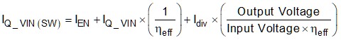
where
- IQ_VIN is the current consumed by the operating (switching) buck converter while unloaded.
- IQ is the current drawn from the VIN terminal. See IQ in Section 8.5.
- IEN is current drawn by the EN terminal. Include this current if EN is connected to VIN. See IEN in Section 8.5. Note that this current drops to a very low value if connected to a voltage less than 5 V.
- Idiv is the current drawn by the feedback voltage divider used to set output voltage.
- ηeff is the light-load efficiency of the buck converter with IQ_VIN removed from the input current of the buck converter. ηeff = 0.8 is a conservative value that can be used under normal operating conditions.