SNVSBA0D February 2020 – August 2021 LM61480-Q1 , LM61495-Q1 , LM62460-Q1
PRODUCTION DATA
- 1 Features
- 2 Applications
- 3 Description
- 4 Revision History
- 5 Device Comparison Table
- 6 Pin Configuration and Functions
- 7 Specifications
-
8 Detailed Description
- 8.1 Overview
- 8.2 Functional Block Diagram
- 8.3
Feature Description
- 8.3.1 Output Voltage Selection
- 8.3.2 Enable EN Pin and Use as VIN UVLO
- 8.3.3 SYNC/MODE Uses for Synchronization
- 8.3.4 Clock Locking
- 8.3.5 Adjustable Switching Frequency
- 8.3.6 RESET Output Operation
- 8.3.7 Internal LDO, VCC UVLO, and BIAS Input
- 8.3.8 Bootstrap Voltage and VCBOOT-UVLO (CBOOT Pin)
- 8.3.9 Adjustable SW Node Slew Rate
- 8.3.10 Spread Spectrum
- 8.3.11 Soft Start and Recovery From Dropout
- 8.3.12 Overcurrent and Short Circuit Protection
- 8.3.13 Hiccup
- 8.3.14 Thermal Shutdown
- 8.4 Device Functional Modes
-
9 Application and Implementation
- 9.1 Application Information
- 9.2
Typical Application
- 9.2.1 Design Requirements
- 9.2.2
Detailed Design Procedure
- 9.2.2.1 Choosing the Switching Frequency
- 9.2.2.2 Setting the Output Voltage
- 9.2.2.3 Inductor Selection
- 9.2.2.4 Output Capacitor Selection
- 9.2.2.5 Input Capacitor Selection
- 9.2.2.6 BOOT Capacitor
- 9.2.2.7 BOOT Resistor
- 9.2.2.8 VCC
- 9.2.2.9 CFF and RFF Selection
- 9.2.2.10 RSPSP Selection
- 9.2.2.11 RT Selection
- 9.2.2.12 RMODE Selection
- 9.2.2.13 External UVLO
- 9.2.2.14 Maximum Ambient Temperature
- 9.2.3 Application Curves
- 10Power Supply Recommendations
- 11Layout
- 12Device and Documentation Support
- 13Mechanical, Packaging, and Orderable Information
Package Options
Mechanical Data (Package|Pins)
- RPH|16
Thermal pad, mechanical data (Package|Pins)
- RPH|16
Orderable Information
8.3.2 Enable EN Pin and Use as VIN UVLO
Apply a voltage less than 0.4 V to the EN pin to put the device into shutdown mode. In shutdown mode, the quiescent current drops to 0.66 µA (typical). Above this voltage but below the LM6x4xx-Q1 lower EN threshold, VCC is active but the SW node remains inactive. Once EN is above VEN, the chip operates normally as long as input voltage is above the minimum operating voltage.
The EN terminal cannot be left floating. The simplest way to enable the operation is to connect the EN pin to VIN. This action allows the self-start-up of the device when VIN drives the internal VCC above its UVLO level. However, many applications benefit from employing an enable divider string, which establishes a precision input undervoltage lockout (UVLO). The precision UVLO can be used for the following:
- Sequencing
- Preventing the device from retriggering when used with long input cables
- Reducing the occurrence of deep discharge of a battery power source
 Figure 8-2 VIN UVLO Using the EN Pin
Resistor values can be calculated using Equation 2:
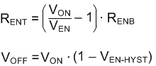
where
- VON = VIN turn-on voltage
- VOFF = VIN turn-off voltage