SNVSB55G February 2019 – September 2022 LM63615-Q1 , LM63625-Q1
PRODUCTION DATA
- 1 Features
- 2 Applications
- 3 Description
- 4 Revision History
- 5 Device Comparison Table
- 6 Pin Configuration and Functions
- 7 Specifications
- 8 Detailed Description
- 9 Application and Implementation
- 10Power Supply Recommendations
- 11Layout
- 12Device and Documentation Support
- 13Mechanical, Packaging, and Orderable Information
Package Options
Mechanical Data (Package|Pins)
Thermal pad, mechanical data (Package|Pins)
Orderable Information
10 Power Supply Recommendations
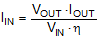
The characteristics of the input supply must be compatible with the limits found in Section 7 of this data sheet. In addition, the input supply must be capable of delivering the required input current to the loaded regulator. The average input current can be estimated with Equation 14.
where
- η is the efficiency
If the regulator is connected to the input supply through long wires or PCB traces, special care is required to achieve good performance. The parasitic inductance and resistance of the input cables can have an adverse effect on the operation of the regulator. The parasitic inductance, in combination with the low-ESR, ceramic input capacitors, can form an under-damped resonant circuit, resulting in overvoltage transients at the input to the regulator. The parasitic resistance can cause the voltage at the VIN pin to dip whenever a load transient is applied to the output. If the application is operating close to the minimum input voltage, this dip can cause the regulator to momentarily shutdown and reset. The best way to solve these kind of issues is to reduce the distance from the input supply to the regulator and use an aluminum or tantalum input capacitor in parallel with the ceramics. The moderate ESR of these types of capacitors help damp the input resonant circuit and reduce any overshoots. A value in the range of 20 µF to 100 µF is usually sufficient to provide input damping and help hold the input voltage steady during large load transients.
It is recommended that the input supply must not be allowed to fall below the output voltage by more than 0.3 V. Under such conditions, the output capacitors discharges through the body diode of the high-side power MOSFET. The resulting current can cause unpredictable behavior, and in extreme cases, possible device damage. If the application allows for this possibility, then use a Schottky diode from VIN to VOUT to provide a path around the regulator for this current.
In some cases, a transient voltage suppressor (TVS) is used on the input of regulators. One class of this device has a snap-back characteristic (thyristor type). The use of a device with this type of characteristic is not recommended. When the TVS fires, the clamping voltage falls to a very low value. If this voltage is less than the output voltage of the regulator, the output capacitors discharges through the device, as mentioned above.
Sometimes, for other system considerations, an input filter is used in front of the regulator. This can lead to instability as well as some of the effects mentioned above, unless it is designed carefully. The AN-2162 Simple Success with Conducted EMI from DCDC Converters User's Guide provides helpful suggestions when designing an input filter for any switching regulator.