SNVSB55G February   2019  – September 2022 LM63615-Q1 , LM63625-Q1

PRODUCTION DATA  

  1. Features
  2. Applications
  3. Description
  4. Revision History
  5. Device Comparison Table
  6. Pin Configuration and Functions
  7. Specifications
    1.     Absolute Maximum Ratings
    2. 7.1 ESD Ratings
    3. 7.2 Recommended Operating Conditions
    4. 7.3 Thermal Information
    5. 7.4 Electrical Characteristics
    6. 7.5 Timing Characteristics
    7. 7.6 Switching Characteristics
    8. 7.7 System Characteristics
    9. 7.8 Typical Characteristics
  8. Detailed Description
    1. 8.1 Overview
    2. 8.2 Functional Block Diagram
    3. 8.3 Feature Description
      1. 8.3.1 Sync/Mode Selection
      2. 8.3.2 Output Voltage Selection
      3. 8.3.3 Switching Frequency Selection
        1. 8.3.3.1 Spread Spectrum Option
      4. 8.3.4 Enable and Start-up
      5. 8.3.5 RESET Flag Output
      6. 8.3.6 Undervoltage Lockout and Thermal Shutdown and Output Discharge
    4. 8.4 Device Functional Modes
      1. 8.4.1 Overview
      2. 8.4.2 Light Load Operation
        1. 8.4.2.1 Sync/FPWM Operation
      3. 8.4.3 Dropout Operation
      4. 8.4.4 Minimum On-time Operation
      5. 8.4.5 Current Limit and Short-Circuit Operation
  9. Application and Implementation
    1. 9.1 Application Information
    2. 9.2 Typical Application
      1. 9.2.1 Design Requirements
      2. 9.2.2 Detailed Design Procedure
        1. 9.2.2.1 Choosing the Switching Frequency
        2. 9.2.2.2 Setting the Output Voltage
          1. 9.2.2.2.1 CFF Selection
        3. 9.2.2.3 Inductor Selection
        4. 9.2.2.4 Output Capacitor Selection
        5. 9.2.2.5 Input Capacitor Selection
        6. 9.2.2.6 CBOOT
        7. 9.2.2.7 VCC
        8. 9.2.2.8 External UVLO
        9. 9.2.2.9 Maximum Ambient Temperature
      3. 9.2.3 Full Feature Design Example
      4. 9.2.4 Application Curves
      5. 9.2.5 EMI Performance Curves
    3. 9.3 What to Do and What Not to Do
  10. 10Power Supply Recommendations
  11. 11Layout
    1. 11.1 Layout Guidelines
      1. 11.1.1 Ground and Thermal Considerations
    2. 11.2 Layout Example
  12. 12Device and Documentation Support
    1. 12.1 Device Support
      1. 12.1.1 Device Nomenclature
    2. 12.2 Documentation Support
      1. 12.2.1 Related Documentation
    3. 12.3 Receiving Notification of Documentation Updates
    4. 12.4 Support Resources
    5. 12.5 Trademarks
    6. 12.6 Glossary
    7. 12.7 Electrostatic Discharge Caution
  13. 13Mechanical, Packaging, and Orderable Information

Package Options

Mechanical Data (Package|Pins)
Thermal pad, mechanical data (Package|Pins)
Orderable Information

Setting the Output Voltage

The output voltage of the LM636x5D-Q1 is set by the condition of the VSEL input. This example requires a 5-V output, so the VSEL input is connected to VCC and the FB input is connected directly to the output capacitor.

For cases where the desired output voltage is other than 5-V or 3.3-V or using the LM636x5C-Q1 variant, an external feedback divider is required. As shown in Figure 9-2, the divider network is comprised of RFBT and RFBB, and closes the loop between the output voltage and the converter. In this case, a 10-kΩ resistor is connected from the VSEL input to ground. The converter regulates the output voltage by holding the voltage on the FB pin equal to the internal reference voltage, 1-V. The resistance of the divider is a compromise between excessive noise pickup and excessive loading of the output. Smaller values of resistance reduce noise sensitivity, but also reduce the light-load efficiency. The recommended value for RFBT is 100 kΩ with a maximum value of 1 MΩ. If 1 MΩ is selected for RFBT, then a feedforward capacitor must be used across this resistor to provide adequate loop phase margin (see Section 9.2.2.2.1). Once RFBT is selected, Equation 5 is used to select RFBB. VREF is nominally 1 V.

Equation 5. GUID-FBFF9D96-2546-43ED-84D8-73EAD8ACB526-low.gif
GUID-DE0F16AF-D7CF-41DA-A747-3EA90E24F416-low.gif
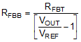
Figure 9-2 Feedback Divider for Adjustable Output Voltage Setting