SNVSCF0 October   2024 LM65680-Q1

ADVANCE INFORMATION  

  1.   1
  2. Features
  3. Applications
  4. Description
  5. Device Comparison Table
  6. Pin Configuration and Functions
  7. Specifications
    1. 6.1 Absolute Maximum Ratings
    2. 6.2 ESD Ratings
    3. 6.3 Recommended Operating Conditions
    4. 6.4 Thermal Information
    5. 6.5 Electrical Characteristics
  8. Detailed Description
    1. 7.1 Overview
    2. 7.2 Functional Block Diagram
    3. 7.3 Feature Descriptions
      1. 7.3.1  Output Voltage Selection
      2. 7.3.2  EN Pin and Use as VIN UVLO
      3. 7.3.3  Device Configuration
      4. 7.3.4  Single-Output Dual-Phase Operation
      5. 7.3.5  Mode Selection
        1. 7.3.5.1 MODE/SYNC Pin Uses for Synchronization
        2. 7.3.5.2 Clock Locking
      6. 7.3.6  Adjustable Switching Frequency
      7. 7.3.7  Dual Random Spread Spectrum (DRSS)
      8. 7.3.8  Internal LDO, VCC UVLO, and BIAS Input
      9. 7.3.9  Bootstrap Voltage (BST Pin)
      10. 7.3.10 Soft Start and Recovery From Dropout
      11. 7.3.11 Safety Features
        1. 7.3.11.1 Power-Good Monitor
        2. 7.3.11.2 Overcurrent and Short-Circuit Protection
        3. 7.3.11.3 Hiccup
        4. 7.3.11.4 Thermal Shutdown
    4. 7.4 Device Functional Modes
      1. 7.4.1 Shutdown Mode
      2. 7.4.2 Active Mode
        1. 7.4.2.1 Peak Current Mode Operation
        2. 7.4.2.2 Auto Mode Operation
          1. 7.4.2.2.1 Diode Emulation
        3. 7.4.2.3 FPWM Mode Operation
  9. Application and Implementation
    1. 8.1 Application Information
      1. 8.1.1 Power Train Components
        1. 8.1.1.1 Buck Inductor
        2. 8.1.1.2 Output Capacitors
        3. 8.1.1.3 Input Capacitors
        4. 8.1.1.4 EMI Filter
      2. 8.1.2 Error Amplifier and Compensation
      3. 8.1.3 Maximum Ambient Temperature
        1. 8.1.3.1 Derating Curves
    2. 8.2 Typical Application
      1. 8.2.1 Design Requirements
      2. 8.2.2 Detailed Design Procedure
        1. 8.2.2.1 Inductor Selection
        2. 8.2.2.2 Output Capacitors
        3. 8.2.2.3 Feed-forward Capacitor (CFF)
        4. 8.2.2.4 Input Capacitor Selection
        5. 8.2.2.5 Choosing the Switching Frequency
        6. 8.2.2.6 Setting the Output Voltage
        7. 8.2.2.7 Compensation Components
        8. 8.2.2.8 CBST
        9. 8.2.2.9 External UVLO
      3. 8.2.3 Application Curves
    3. 8.3 Best Design Practices
    4. 8.4 Power Supply Recommendations
    5. 8.5 Layout
      1. 8.5.1 Layout Guidelines
        1. 8.5.1.1 Ground and Thermal Considerations
      2. 8.5.2 Layout Example
  10. Device and Documentation Support
    1. 9.1 Development Support
    2. 9.2 Documentation Support
      1. 9.2.1 Related Documentation
        1. 9.2.1.1 PCB Layout Resources
        2. 9.2.1.2 Thermal Design Resources
    3. 9.3 Receiving Notification of Documentation Updates
    4. 9.4 Support Resources
    5. 9.5 Trademarks
    6. 9.6 Electrostatic Discharge Caution
    7. 9.7 Glossary
  11. 10Revision History
  12. 11Mechanical, Packaging, and Orderable Information
    1. 11.1 Tape and Reel Information

Package Options

Mechanical Data (Package|Pins)
Thermal pad, mechanical data (Package|Pins)
Orderable Information
Diode Emulation

Diode emulation prevents reverse current though the inductor, which requires a lower frequency needed to regulate given a fixed peak inductor current. Diode emulation also limits ripple current as frequency is reduced. Frequency reduces when peak inductor current goes below IPEAK-MIN. With a fixed peak current, as output current is reduced to zero, frequency must be reduced to near zero to maintain regulation.
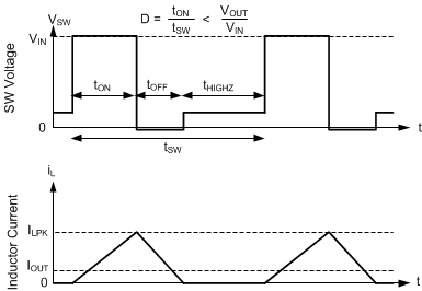
LM65680-Q1 PFM Operation
In auto mode, the low-side device is turned off after inductor current is near zero. As a result, after output current is less than half of inductor ripple in CCM, the part operates in DCM. This action is equivalent to saying that diode emulation is active.
Figure 7-11 PFM Operation

The LM656x0-Q1 has a minimum peak inductor current setting in auto mode. That being said, when current is reduced to a low value with fixed input voltage, on-time is constant. Regulation is then achieved by adjusting frequency. This mode of operation is called PFM mode regulation.