SNOS879I August 1999 – May 2016 LM7301
PRODUCTION DATA.
- 1 Features
- 2 Applications
- 3 Description
- 4 Revision History
- 5 Pin Configuration and Functions
- 6 Specifications
- 7 Detailed Description
- 8 Applications and Implementation
- 9 Power Supply Recommendations
- 10Layout
- 11Device and Documentation Support
- 12Mechanical, Packaging, and Orderable Information
Package Options
Mechanical Data (Package|Pins)
Thermal pad, mechanical data (Package|Pins)
Orderable Information
7 Detailed Description
7.1 Overview
Low supply current, wide bandwidth, input common mode voltage range that includes both rails, rail-to-rail output, good capacitive load driving ability, wide supply voltage (1.8 V to 32 V), and low distortion all make the LM7301 ideal for many diverse applications.
The high common-mode rejection ratio and full rail-to-rail input range provides precision performance when operated in noninverting applications where the common-mode error is added directly to the other system errors.
7.2 Feature Description
7.2.1 Capacitive Load Driving
The LM7301 has the ability to drive large capacitive loads. For example, 1000 pF only reduces the phase margin to about 25°.
7.2.2 Transient Response
The LM7301 offers a very clean, well-behaved transient response. Figure 19, Figure 20, Figure 22, and Figure 23 show the response when operated at gains of +1 and −1 when handling both small and large signals. The large phase margin, typically 70° to 80°, assures clean and symmetrical response. In the large signal scope photos, Figure 19 and Figure 22, the input signal is set to 4.8 V. The output goes to within 100 mV of the supplies cleanly and without overshoot. In the small signal samples, the response is clean, with only slight overshoot when used as a follower. Figure 21 and Figure 24 are the circuits used to make these photos.
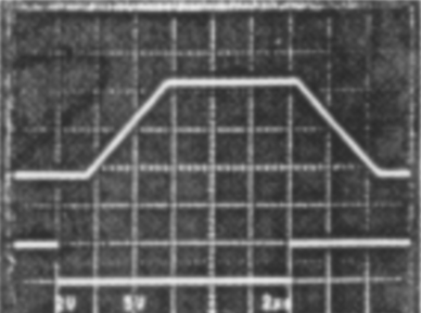 Figure 19. AV = –1 V/V, Large Signal Behavior (1 V/div,
 2 µs/div)
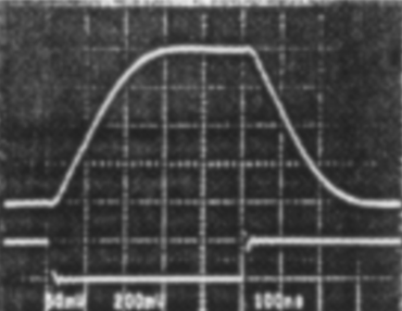 Figure 20. AV = –1 V/V, Small Signal Behavior (0.2 V/div, 100 µs/div)
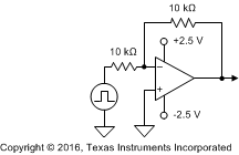 Figure 21. AV = –1 V/V Schematic
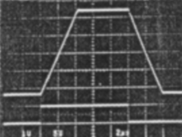 Figure 22. AV = 1 V/V, Large Signal Behavior (1 V/div,
2 us/div)
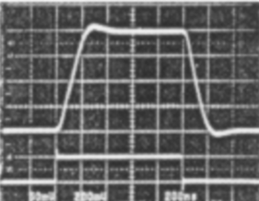 Figure 23. AV = 1 V/V, Small Signal Behavior (0.2 V/div,
200 µs/div)
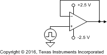 Figure 24. AV = 1-V/V Schematic
7.2.3 Wide Supply Range
The high power-supply rejection ratio (PSRR) and common-mode rejection ratio (CMRR) provide precision performance when operated on battery or other unregulated supplies. This advantage is further enhanced by the very wide supply range (2.2 V to 30 V, ensured) offered by the LM7301. In situations where highly variable or unregulated supplies are present, the excellent PSRR and wide supply range of the LM7301 benefit the system designer with continued precision performance, even in such adverse supply conditions.
7.2.4 Specific Advantages of 5-Pin SOT-23 (TinyPak)
The obvious advantage of the 5-pin SOT-23, TinyPak, is that it can save board space, a critical aspect of any portable or miniaturized system design. The need to decrease overall system size is inherent in any handheld, portable, or lightweight system application.
Furthermore, the low profile can help in height limited designs, such as consumer hand-held remote controls, sub-notebook computers, and PCMCIA cards.
An additional advantage of the tiny package is that it allows better system performance due to ease of package placement. Because the tiny package is so small, it can fit on the board right where the operational amplifier must be placed for optimal performance, unconstrained by the usual space limitations. This optimal placement of the tiny package allows for many system enhancements that are not easily achieved with the constraints of a larger package. For example, problems such as system noise due to undesired pickup of digital signals can be easily reduced or mitigated. This pickup problem is often caused by long wires in the board layout going to or from an operational amplifier. By placing the tiny package closer to the signal source and allowing the LM7301 output to drive the long wire, the signal becomes less sensitive to such pickup. An overall reduction of system noise results.
Often times system designers try to save space by using dual or quad op amps in their board layouts. This causes a complicated board layout due to the requirement of routing several signals to and from the same place on the board. Using the tiny operational amplifier eliminates this problem.
Additional space savings parts are available in tiny packages from Texas Instruments, including low-power amplifiers, precision-voltage references, and voltage regulators.
7.2.5 Low-Distortion, High-Output Drive Capability
The LM7301 offers superior low-distortion performance, with a total-harmonic-distortion-plus-noise of 0.06% at f = 10 kHz. The advantage offered by the LM7301 is its low distortion levels, even at high output current and low load resistance. See Stability Considerations for methods used to ensure stability under all load conditions.
7.3 Device Functional Modes
7.3.1 Stability Considerations
Rail-to-rail output amplifiers like the LM7301 use the collector of the drive transistor(s) at the output pin, as shown in Figure 25. This allows the load to be driven as close as possible towards either supply rail.
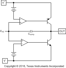 Figure 25. Simplified Output Stage Block Diagram
While this architecture maximizes the load voltage swing range, it increases the dependence of loop gain and subsequently stability, on load impedance and DC load current, compared to a non-rail-to-rail architecture. Thus, with this type of output stage, it is even more crucial to ensure stability by meticulous bench verification under all load conditions, and to apply the necessary compensation or circuit modifications to overcome any instability, if necessary. Any such bench verification should also include temperature, supply voltage, input common mode and output bias point variations as well as capacitive loading.
For example, one set of conditions for which stability of the LM7301 amplifier may be compromised is when the DC output load is larger than ±0.5 mA, with input and output biased to mid-rail. Under such conditions, it may be possible to observe open-loop gain response peaking at a high frequency (for example, 200 MHz), which is beyond the expected frequency range of the LM7301 (4 MHz GBW). Without taking any precautions against gain peaking, it is possible to see increased settling time or even oscillations, especially with low closed loop gain and / or light AC loading. It is possible to reduce or eliminate this gain peaking by using external compensation components. One possible scheme that can be applied to reduce or eliminate this gain peaking is shown in Figure 26.
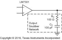 Figure 26. Non-Dissipating Snubber Network to Reduce Gain Peaking
The non-dissipating snubber, consisting of Rc and Cc, acts as AC load to reduce high-frequency gain peaking with no DC loading so that total power dissipation is not increased. The increased AC load effectively reduces loop gain at higher frequencies thereby reducing gain peaking due to the possible causes stated in the previous sentence. For the particular set of Rc and Cc values shown in Figure 26, loop gain peaking is reduced by about 25 dB under worst case peaking conditions (I_source= 2mA DC at around 180 MHz) thus confining loop gain to less than 0 dB and eliminating any possible instability. For best results, it may be necessary to tune the values of Rc and Cc in a particular application to consider other subtleties and tolerances.
7.3.2 Power Dissipation
Although the LM7301 has internal output current limiting, shorting the output to ground when operating on a 30-V power supply will cause the operational amplifier to dissipate about 350 mW. This is a worst-case example. In the 8-pin SOIC package, this will cause a temperature rise of 42°C. In the 5-pin SOT-23 package, the higher thermal resistance will cause a calculated rise of 59°C. This can raise the junction temperature to greater than the absolute maximum temperature of 150°C.
Operating from split supplies greatly reduces the power dissipated when the output is shorted. Operating on
±15-V supplies can only cause a temperature rise of 21°C in the 8-pin SOIC and 30°C in the 5-pin SOT-23 package, assuming the short is to ground.