SNOSDC0A October 2020 – December 2020 LM7310
PRODUCTION DATA
- 1 Features
- 2 Applications
- 3 Description
- 4 Revision History
- 5 Pin Configuration and Functions
- 6 Specifications
-
7 Detailed Description
- 7.1 Overview
- 7.2 Functional Block Diagram
- 7.3
Feature Description
- 7.3.1 Input Reverse Polarity Protection
- 7.3.2 Undervoltage Protection (UVLO & UVP)
- 7.3.3 Overvoltage Lockout (OVLO)
- 7.3.4 Inrush Current control and Fast-trip
- 7.3.5 Analog Load Current Monitor Output
- 7.3.6 Reverse Current Protection
- 7.3.7 Overtemperature Protection (OTP)
- 7.3.8 Fault Response
- 7.3.9 Power Good Indication (PG)
- 7.4 Device Functional Modes
- 8 Application and Implementation
- 9 Power Supply Recommendations
- 10Layout
- 11Device and Documentation Support
- 12Mechanical, Packaging, and Orderable Information
Package Options
Mechanical Data (Package|Pins)
- RPW|10
Thermal pad, mechanical data (Package|Pins)
Orderable Information
3 Description
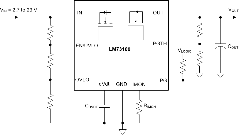
The LM73100 is a highly integrated circuit protection and power management solution in a small package. The device provides multiple protection modes using very few external components and is a robust defense against voltage surges, reverse polarity, reverse current and excessive inrush current.
With integrated back-to-back FETs, reverse current flow from output to input is blocked at all times, making the device well suited for power MUX/ORing applications. The device uses linear ORing based scheme to ensure almost zero DC reverse current and emulates ideal diode behavior with minimum forward voltage drop and power dissipation.
Applications with particular inrush current requirements can set the output slew rate with a single external capacitor. Loads are protected from input overvoltage conditions by cutting off the output if input exceeds an adjustable overvoltage threshold. The device also provides fast trip response to transient overcurrent events during steady state.
The device provides an accurate sense of the output load current on the analog current monitor pin.
The device is available in a 2-mm x 2-mm, 10-pin HotRod QFN package for improved thermal performance and reduced system footprint.
The device is characterized for operation over a junction temperature range of –40°C to +125°C.
| PART NUMBER | PACKAGE(1) | BODY SIZE (NOM) |
|---|---|---|
| LM73100RPW | QFN (10) | 2 mm x 2 mm |
 Simplified Schematic