SNOSDC0A October 2020 – December 2020 LM7310
PRODUCTION DATA
- 1 Features
- 2 Applications
- 3 Description
- 4 Revision History
- 5 Pin Configuration and Functions
- 6 Specifications
-
7 Detailed Description
- 7.1 Overview
- 7.2 Functional Block Diagram
- 7.3
Feature Description
- 7.3.1 Input Reverse Polarity Protection
- 7.3.2 Undervoltage Protection (UVLO & UVP)
- 7.3.3 Overvoltage Lockout (OVLO)
- 7.3.4 Inrush Current control and Fast-trip
- 7.3.5 Analog Load Current Monitor Output
- 7.3.6 Reverse Current Protection
- 7.3.7 Overtemperature Protection (OTP)
- 7.3.8 Fault Response
- 7.3.9 Power Good Indication (PG)
- 7.4 Device Functional Modes
- 8 Application and Implementation
- 9 Power Supply Recommendations
- 10Layout
- 11Device and Documentation Support
- 12Mechanical, Packaging, and Orderable Information
Package Options
Mechanical Data (Package|Pins)
- RPW|10
Thermal pad, mechanical data (Package|Pins)
Orderable Information
8.5 USB PD Port Protection
End equipments like PC, Notebooks, Docking Stations, Monitors etc. have USB PD ports which can be configured as DFP (Source), UFP (Sink) or DRP (Source+Sink). LM73100 can be used independently or in conjunction with TPS259470x to handle the power path protection requirements of USB PD ports as shown in Figure 8-11 below.
LM73100 provides overvoltage protection on the sink path, while blocking reverse current from internal sink rail to the port.
TPS259470x provides overcurrent & short-circuit protection in the source path, while blocking any reverse current from the port to the internal source power rail. The fast recovery from reverse current blocking ensures minimum supply droop during Fast Role Swap (FRS) events. The PD controller can also use the OVLO pin as an active low enable signal to control the power path. Holding the OVLO pin high keeps the device in OFF state in sink mode and blocks current in both directions. Once the PD controller determines the need to start sourcing power, it can pull the OVLO pin low to trigger a fast recovery from OFF to ON state, meeting the FRS timing requirements.
 Figure 8-11 USB PD Port Protection
The linear ORing mechanism in TPS259470x & LM73100 ensures that there's no reverse current flowing from one power source to the other during fast or slow ramp of either supply.
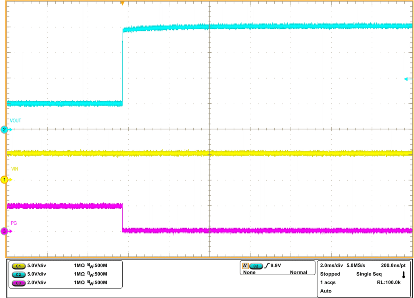
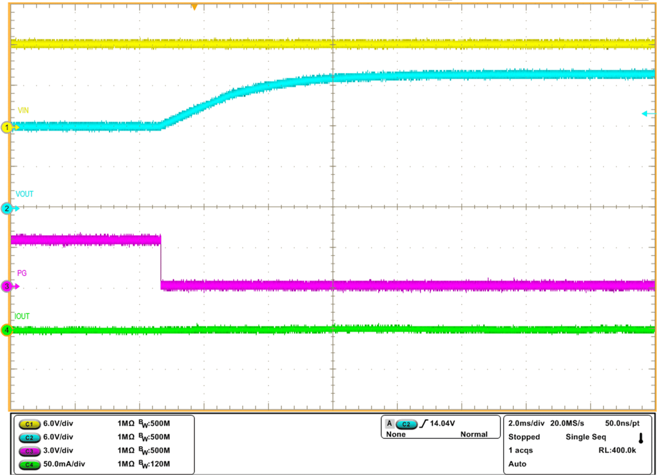
The following waveforms illustrate the LM73100 reverse current blocking behavior in USB applications.
 Figure 8-12 LM73100 Reverse Current Protection During 20-V Hot-Plug at Output
 Figure 8-13 LM73100 Reverse Current Protection During 20-V Voltage Ramp at Output