SNVSB12B November 2017 – May 2021 LM73605-Q1 , LM73606-Q1
PRODUCTION DATA
- 1 Features
- 2 Applications
- 3 Description
- 4 Revision History
- 5 Device Comparison
- 6 Pin Configuration and Functions
- 7 Specifications
-
8 Detailed Description
- 8.1 Overview
- 8.2 Functional Block Diagram
- 8.3
Feature Description
- 8.3.1 Synchronous Step-Down Regulator
- 8.3.2 Auto Mode and FPWM Mode
- 8.3.3 Fixed-Frequency Peak Current-Mode Control
- 8.3.4 Adjustable Output Voltage
- 8.3.5 Enable and UVLO
- 8.3.6 Internal LDO, VCC_UVLO, and BIAS Input
- 8.3.7 Soft Start and Voltage Tracking
- 8.3.8 Adjustable Switching Frequency
- 8.3.9 Frequency Synchronization and Mode Setting
- 8.3.10 Internal Compensation and CFF
- 8.3.11 Bootstrap Capacitor and VBOOT-UVLO
- 8.3.12 Power-Good and Overvoltage Protection
- 8.3.13 Overcurrent and Short-Circuit Protection
- 8.3.14 Thermal Shutdown
- 8.4 Device Functional Modes
- 9 Layout
- 10Device and Documentation Support
Package Options
Mechanical Data (Package|Pins)
- RNP|30
Thermal pad, mechanical data (Package|Pins)
- RNP|30
Orderable Information
8.3.5 Enable and UVLO
The LM73605-Q1/6-Q1 output voltage when the VCC voltage is higher than the undervoltage lock out (UVLO) level, VCC_UVLO, and the EN voltage is higher than VEN_VOUT_H.
The internal LDO output voltage VCC is turned on when the EN voltage is higher than VEN_VCC_H. The precision enable circuitry is also turned on when VCC is above UVLO. Normal operation of the LM73605-Q1/6-Q1 with regulated output voltage is enabled when the EN voltage is greater than VEN_VOUT_H. When the EN voltage is less than VEN_VCC_L, the device is in shutdown mode. The internal dividers make sure VEN_VOUT_H is always higher than VEN_VCC_H.
The EN pin cannot be left floating. The simplest way to enable the operation of the LM73605-Q1/6-Q1 is to connect the EN pin to PVIN, which allows self-start-up of the LM73605-Q1/6-Q1 when VIN rises. Use of a pullup resistor between PVIN and EN pins helps reduce noise coupling from PVIN pin to the EN pin.
Many applications benefit from employing an enable divider to establish a customized system UVLO. This can be used either for sequencing, system timing requirement, or to reduce the occurrence of deep discharge of a battery power source. Figure 8-5 shows how to use a resistor divider to set a system UVLO level. An external logic output can also be used to drive the EN pin for system sequencing.
 Figure 8-5 System UVLO
With a selected RENT, the RENB can be calculated by:
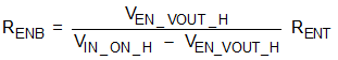
where
- VIN_ON_H is the desired supply voltage threshold to turn on this device
Note that the divider adds to supply quiescent current by VIN / (RENT + RENB). Small RENT and RENB values add more quiescent current loss. However, large divider values make the node more sensitive to noise. RENT in the hundreds of kΩ range is a good starting point.