SNVSB12B November 2017 – May 2021 LM73605-Q1 , LM73606-Q1
PRODUCTION DATA
- 1 Features
- 2 Applications
- 3 Description
- 4 Revision History
- 5 Device Comparison
- 6 Pin Configuration and Functions
- 7 Specifications
-
8 Detailed Description
- 8.1 Overview
- 8.2 Functional Block Diagram
- 8.3
Feature Description
- 8.3.1 Synchronous Step-Down Regulator
- 8.3.2 Auto Mode and FPWM Mode
- 8.3.3 Fixed-Frequency Peak Current-Mode Control
- 8.3.4 Adjustable Output Voltage
- 8.3.5 Enable and UVLO
- 8.3.6 Internal LDO, VCC_UVLO, and BIAS Input
- 8.3.7 Soft Start and Voltage Tracking
- 8.3.8 Adjustable Switching Frequency
- 8.3.9 Frequency Synchronization and Mode Setting
- 8.3.10 Internal Compensation and CFF
- 8.3.11 Bootstrap Capacitor and VBOOT-UVLO
- 8.3.12 Power-Good and Overvoltage Protection
- 8.3.13 Overcurrent and Short-Circuit Protection
- 8.3.14 Thermal Shutdown
- 8.4 Device Functional Modes
- 9 Layout
- 10Device and Documentation Support
Package Options
Mechanical Data (Package|Pins)
- RNP|30
Thermal pad, mechanical data (Package|Pins)
- RNP|30
Orderable Information
3 Description
The LM73605-Q1/LM73606-Q1 family of devices are easy-to-use synchronous step-down DC/DC converters capable of driving up to 5 A (LM73605-Q1) or 6 A (LM73606-Q1) of load current from a supply voltage ranging from 3.5 V to 36 V. The LM73605-Q1/LM73606-Q1 provide exceptional efficiency and output accuracy in a very small solution size. Peak current-mode control is employed. Additional features such as adjustable switching frequency, synchronization to an external clock, power-good flag, precision enable, adjustable soft start, and tracking provide both flexible and easy-to-use solutions for a wide range of applications. Automatic frequency foldback at light load and optional external bias improve efficiency over the entire load range. The family requires few external components and has a pinout designed for simple PCB layout with optimal EMI and thermal performance. Protection features include thermal shutdown, input undervoltage lookout, cycle-cy-cycle current limiting, and hiccup short-citcuit protection. The LM73605-Q1 and LM73606-Q1 devices are pin-to-pin compatible for easy current scaling.
| PART NUMBER | PACKAGE | BODY SIZE (NOM) |
|---|---|---|
| LM73605-Q1 | WQFN (30) Wettable and non-wettable flanks |
6.00 mm × 4.00 mm |
| LM73606-Q1 |
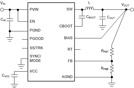
 Simplified Schematic
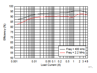
 Efficiency versus Load
Current VOUT = 5 V, VIN = 12 V, Auto Mode