SNVSAH5A September 2017 – May 2020 LM73605 , LM73606
PRODUCTION DATA.
- 1 Features
- 2 Applications
- 3 Description
- 4 Revision History
- 5 Pin Configuration and Functions
- 6 Specifications
-
7 Detailed Description
- 7.1 Overview
- 7.2 Functional Block Diagram
- 7.3
Feature Description
- 7.3.1 Synchronous Step-Down Regulator
- 7.3.2 Auto Mode and FPWM Mode
- 7.3.3 Fixed-Frequency Peak Current-Mode Control
- 7.3.4 Adjustable Output Voltage
- 7.3.5 Enable and UVLO
- 7.3.6 Internal LDO, VCC_UVLO, and BIAS Input
- 7.3.7 Soft Start and Voltage Tracking
- 7.3.8 Adjustable Switching Frequency
- 7.3.9 Frequency Synchronization and Mode Setting
- 7.3.10 Internal Compensation and CFF
- 7.3.11 Bootstrap Capacitor and VBOOT-UVLO
- 7.3.12 Power-Good and Overvoltage Protection
- 7.3.13 Overcurrent and Short-Circuit Protection
- 7.3.14 Thermal Shutdown
- 7.4 Device Functional Modes
-
8 Application and Implementation
- 8.1 Application Information
- 8.2
Typical Application
- 8.2.1 Design Requirements
- 8.2.2
Detailed Design Procedure
- 8.2.2.1 Custom Design With WEBENCH® Tools
- 8.2.2.2 Output Voltage Setpoint
- 8.2.2.3 Switching Frequency
- 8.2.2.4 Input Capacitors
- 8.2.2.5 Inductor Selection
- 8.2.2.6 Output Capacitor Selection
- 8.2.2.7 Feedforward Capacitor
- 8.2.2.8 Bootstrap Capacitors
- 8.2.2.9 VCC Capacitor
- 8.2.2.10 BIAS
- 8.2.2.11 Soft Start
- 8.2.2.12 Undervoltage Lockout Setpoint
- 8.2.2.13 PGOOD
- 8.2.3 Application Curves
- 9 Power Supply Recommendations
- 10Layout
- 11Device and Documentation Support
- 12Mechanical, Packaging, and Orderable Information
Package Options
Mechanical Data (Package|Pins)
- RNP|30
Thermal pad, mechanical data (Package|Pins)
- RNP|30
Orderable Information
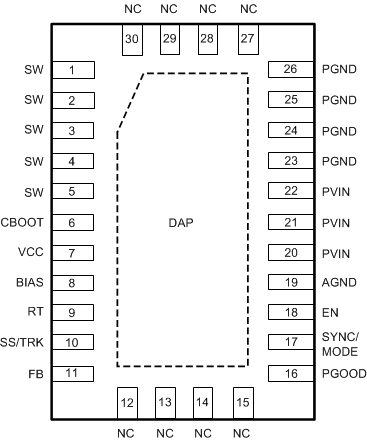
5 Pin Configuration and Functions
RNP Package
30-Pin Wettable Flanks QFN (WQFN) 6 mm × 4 mm × 0.8 mm
Top View

Pin Functions
| PIN | I/O(1) | DESCRIPTION | |
|---|---|---|---|
| NO. | NAME | ||
| 1, 2, 3, 4, 5 | SW | P | Switching output of the regulator. Internally connected to source of the HS FET and drain of the LS FET. Connect to power inductor and bootstrap capacitor. |
| 6 | CBOOT | P | Bootstrap capacitor connection for HS FET driver. Connect a high-quality 470-nF capacitor from this pin to the SW pin. |
| 7 | VCC | P | Output of internal bias supply. Used as supply to internal control circuits and drivers. Connect a high-quality 2.2-µF capacitor from this pin to GND. TI does not recommend loading this pin by external circuitry. |
| 8 | BIAS | P | Optional BIAS LDO supply input. TI recommends tying to VOUT when 3.3 V ≤ VOUT ≤ 18 V, or tie to an external 3.3-V or 5-V rail if available, to improve efficiency. BIAS pin voltage must not be greater than VIN. Tie to ground when not in use. |
| 9 | RT | A | Switching frequency setting pin. Place a resistor from this pin to ground to set the switching frequency. If floating, the default switching frequency is 500 kHz. Do not short to ground. |
| 10 | SS/TRK | A | Soft-start control pin. Leave this pin floating for a fixed internal soft-start ramp. An external capacitor can be connected from this pin to ground to extend the soft start time. A 2-µA current sourced from this pin charges the capacitor to provide the ramp. Connect to external ramp for tracking. Do not short to ground. |
| 11 | FB | I | Feedback input for output voltage regulation. Connect a resistor divider to set the output voltage. Never short this pin to ground during operation. |
| 12–15, 27–30 | NC | — | No internal connection. Connect to ground net and copper to improve heat sinking and board-level reliability. |
| 16 | PGOOD | O | Open drain power-good flag output. Connect to suitable voltage supply through a current limiting resistor. High = VOUT regulation OK, Low = VOUT regulation fault. PGOOD = LOW when EN = low and VIN > 2 V. |
| 17 | SYNC/MODE | I | Synchronization input and mode setting pin. Do not float. Tie to ground if not used.
Tie to ground: auto mode, higher efficiency at light loads; Tie to logic high: forced PWM, constant switching frequency over load; Tie to external clock source: forced PWM, synchronize to the rising edge of the external clock. |
| 18 | EN | I | Enable input to regulator. Do not float. High = ON, Low = OFF. Can be tied to PVIN. Precision enable input allows adjustable input voltage UVLO using external resistor divider. |
| 19 | AGND | G | Analog ground. Ground reference for internal circuitry. All electrical parameters are measured with respect to this pin. Connect to system ground on PCB. |
| 20–22 | PVIN | P | Supply input to internal bias LDO and HS FET. Connect to input supply and input bypass capacitors CIN. CIN must be placed right next to this pin and PGND pins on PCB, and connected with short and wide traces. |
| 23–26 | PGND | G | Power ground, connected to the source of LS FET internally. Connect to system ground, DAP/EP, AGND, ground side of CIN and COUT on PCB. Path to CIN must be as short as possible |
| EP | DAP | G | Low impedance connection to AGND. Connect to system ground on PCB. Major heat dissipation path for the device. Must be used for heat sinking by soldering to ground copper on PCB. Thermal vias are preferred to improve heat dissipation to other layers. |
(1) A = Analog, O = Output, I = Input, G = Ground, P = Power