SNVSB12B November 2017 – May 2021 LM73605-Q1 , LM73606-Q1
PRODUCTION DATA
- 1 Features
- 2 Applications
- 3 Description
- 4 Revision History
- 5 Device Comparison
- 6 Pin Configuration and Functions
- 7 Specifications
-
8 Detailed Description
- 8.1 Overview
- 8.2 Functional Block Diagram
- 8.3
Feature Description
- 8.3.1 Synchronous Step-Down Regulator
- 8.3.2 Auto Mode and FPWM Mode
- 8.3.3 Fixed-Frequency Peak Current-Mode Control
- 8.3.4 Adjustable Output Voltage
- 8.3.5 Enable and UVLO
- 8.3.6 Internal LDO, VCC_UVLO, and BIAS Input
- 8.3.7 Soft Start and Voltage Tracking
- 8.3.8 Adjustable Switching Frequency
- 8.3.9 Frequency Synchronization and Mode Setting
- 8.3.10 Internal Compensation and CFF
- 8.3.11 Bootstrap Capacitor and VBOOT-UVLO
- 8.3.12 Power-Good and Overvoltage Protection
- 8.3.13 Overcurrent and Short-Circuit Protection
- 8.3.14 Thermal Shutdown
- 8.4 Device Functional Modes
- 9 Layout
- 10Device and Documentation Support
Package Options
Mechanical Data (Package|Pins)
- RNP|30
Thermal pad, mechanical data (Package|Pins)
- RNP|30
Orderable Information
9.1.3 Optimize Thermal Performance
The key to thermal optimization on PCB design is to provide heat transferring paths from the device to the outer large copper area. Use thick copper (2 oz) on high current layer or layers if possible. Use thermal vias under the DAP to transfer heat to other layers. Connect NC pins to the GND net, so that GND copper can run underneath the device to create dog-bone shaped heat sink. Try to leave copper solid on IC side as much as possible above and below the device. Place components and route traces away from major heat transferring paths if possible, to avoid blocking heat dissipation path. Try to leave copper solid, free of components and traces, around the thermal vias on the other side of the board as well. Solid copper behaves as heat sink to spread the heat to a larger area and provide more contact area to the air.
When calculating power dissipation, use the maximum input voltage and the average output current for the application. Many common operating conditions are provided in the Section 9.2.3. Less common applications can be derived through interpolation. In all designs, the junction temperature must be kept below the rated maximum of 125°C.
The thermal characteristics of the LM73605-Q1/6-Q1 are specified using the parameter RθJA, which characterize thermal resistance from the junction of the silicon to the ambient in a specific system. Although the value of RθJA is dependant on many variables, it still can be used to approximate the operating junction temperature of the device. To obtain an estimate of the device junction temperature, you can use Equation 30:
where
- TJ = Junction temperature in °C
- PIC_LOSS = VIN × IIN × (1 − efficiency) − 1.1 × IOUT × DCR
- DCR = Inductor DC parasitic resistance in Ω
- RθJA = Junction-to-ambient thermal resistance of the device in °C/W
- TA = Ambient temperature in °C.
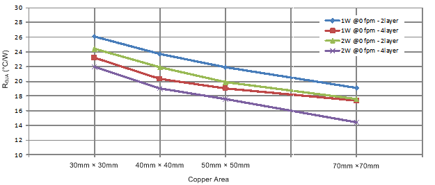
The maximum operating junction temperature of the LM73605-Q1/6-Q1 is 125°C. RθJA is highly related to PCB size and layout, as well as environmental factors such as heat sinking and air flow. Figure 9-2 shows measured results of RθJA with different copper area on 2-layer boards and 4-layer boards, with 1-W and 2-W power dissipation on the LM73605-Q1/6-Q1.
 Figure 9-2 Measured RθJA versus PCB Copper Area on 2-Layer Boards and 4-Layer Boards