SNOSDD6 September 2021 LM74700-EP
PRODUCTION DATA
- 1 Features
- 2 Applications
- 3 Description
- 4 Revision History
- 5 Pin Configuration and Functions
- 6 Specifications
- 7 Parameter Measurement Information
- 8 Detailed Description
-
9 Application and Implementation
- 9.1 Application Information
- 9.2 Typical Application
- 9.3 OR-ing Application Configuration
- 10Power Supply Recommendations
- 11Layout
- 12Device and Documentation Support
- 13Mechanical, Packaging, and Orderable Information
Package Options
Mechanical Data (Package|Pins)
- DDF|8
Thermal pad, mechanical data (Package|Pins)
Orderable Information
5 Pin Configuration and Functions
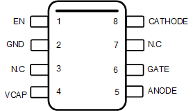
 Figure 5-1 DDF Package8-Pin SOT-23Top View
Table 5-1 Pin Functions
| PIN | I/O(1) | DESCRIPTION | |
|---|---|---|---|
| NO. | NAME | ||
| 1 | EN | I | Enable pin. Can be connected to ANODE for always ON operation. |
| 2 | GND | G | Ground pin |
| 3 | N.C | No connection. Keep this pin floating. | |
| 4 | VCAP | O | Charge pump output. Connect to external charge pump capacitor. |
| 5 | ANODE | I | Anode of the diode and input power. Connect to the source of the external N-channel MOSFET. |
| 6 | GATE | O | Gate drive output. Connect to gate of the external N-channel MOSFET. |
| 7 | N.C | No connection. Keep this pin floating. | |
| 8 | CATHODE | I | Cathode of the diode. Connect to the drain of the external N-channel MOSFET. |
(1) I = Input, O = Output, G = GND