SNOSD17G October 2017 – December 2020 LM74700-Q1
PRODMIX
- 1 Features
- 2 Applications
- 3 Description
- 4 Revision History
- 5 Pin Configuration and Functions
- 6 Specifications
- 7 Typical Characteristics
- 8 Parameter Measurement Information
- 9 Detailed Description
-
10Application and Implementation
- 10.1 Application Information
- 10.2 OR-ing Application Configuration
- 11Power Supply Recommendations
- 12Layout
- 13Device and Documentation Support
- 14Mechanical, Packaging, and Orderable Information
Package Options
Mechanical Data (Package|Pins)
Thermal pad, mechanical data (Package|Pins)
Orderable Information
7 Typical Characteristics
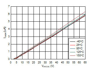 Figure 7-1 Shutdown Supply Current vs Supply Voltage
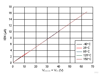 Figure 7-3 Enable Sink Current vs Supply Voltage
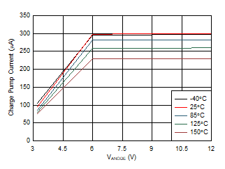 Figure 7-5 Charge Pump Current vs Supply Voltage at VCAP = 6 V
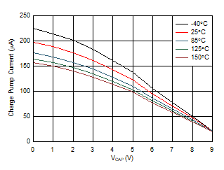 Figure 7-7 Charge Pump V-I Characteristics at VANODE = 3.2 V
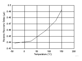 Figure 7-9 Reverse Current Blocking Delay vs Temperature
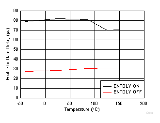 Figure 7-11 Enable to Gate Delay vs Temperature
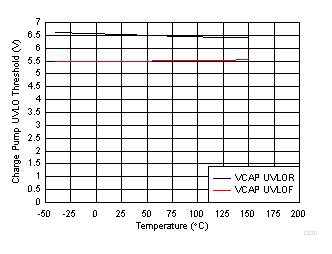 Figure 7-13 Charge Pump UVLO Threshold vs Temperature
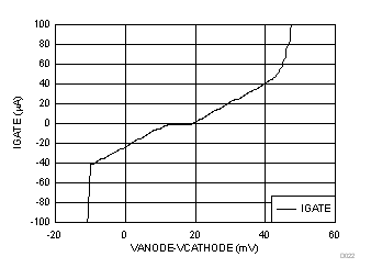 Figure 7-15 Gate
Current vs Forward Voltage Drop
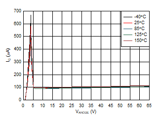 Figure 7-2 Operating Quiescent Current vs Supply Voltage
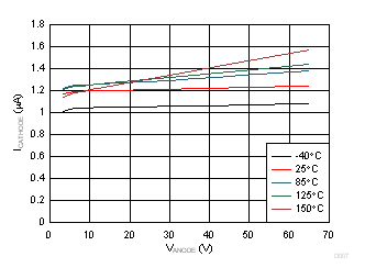 Figure 7-4 CATHODE Sink Current vs Supply Voltage
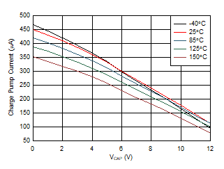 Figure 7-6 Charge Pump V-I Characteristics at VANODE > = 12 V
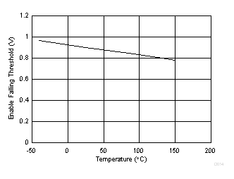 Figure 7-8 Enable Falling Threshold vs Temperature
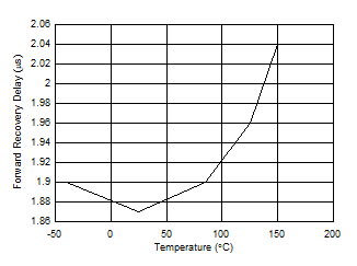 Figure 7-10 Forward Recovery Delay vs Temperature
 Figure 7-12 Charge Pump ON/OFF Threshold vs Temperature
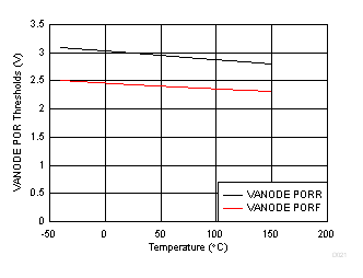 Figure 7-14 VANODE POR Threshold vs Temperature