SNOSDD9 December   2022 LM7481

PRODUCTION DATA  

  1. Features
  2. Applications
  3. Description
  4. Revision History
  5. Pin Configuration and Functions
  6. Specifications
    1. 6.1 Absolute Maximum Ratings
    2. 6.2 ESD Ratings
    3. 6.3 Recommended Operating Conditions
    4. 6.4 Thermal Information
    5. 6.5 Electrical Characteristics
    6. 6.6 Switching Characteristics
    7. 6.7 Typical Characteristics
  7. Parameter Measurement Information
  8. Detailed Description
    1. 8.1 Overview
    2. 8.2 Functional Block Diagram
    3. 8.3 Feature Description
      1. 8.3.1 Charge Pump
      2. 8.3.2 Dual Gate Control (DGATE, HGATE)
        1. 8.3.2.1 Reverse Battery Protection (A, C, DGATE)
        2. 8.3.2.2 Load Disconnect Switch Control (HGATE, OUT)
      3. 8.3.3 Overvoltage Protection and Battery Voltage sensing (VSNS, SW, OV)
      4. 8.3.4 Low Iq Shutdown and Undervoltage Lockout (EN/UVLO)
    4. 8.4 Device Functional Modes
    5. 8.5 Application Examples
      1. 8.5.1 Redundant Supply OR-ing With Inrush Current Limiting, Overvoltage Protection and ON/OFF Control
  9. Application and Implementation
    1. 9.1 Application Information
    2. 9.2 Typical 12-V Reverse Battery Protection Application
      1. 9.2.1 Design Requirements for 12-V Battery Protection
      2. 9.2.2 Automotive Reverse Battery Protection
      3. 9.2.3 Detailed Design Procedure
        1. 9.2.3.1 Design Considerations
        2. 9.2.3.2 Charge Pump Capacitance VCAP
        3. 9.2.3.3 Input and Output Capacitance
        4. 9.2.3.4 Hold-up Capacitance
        5. 9.2.3.5 Overvoltage Protection and Battery Monitor
      4. 9.2.4 MOSFET Selection: Blocking MOSFET Q1
      5. 9.2.5 MOSFET Selection: Hot-Swap MOSFET Q2
      6. 9.2.6 TVS selection
      7. 9.2.7 Application Curves
    3. 9.3 Do's and Don'ts
    4. 9.4 Power Supply Recommendations
      1. 9.4.1 Transient Protection
      2. 9.4.2 TVS Selection for 12-V Battery Systems
      3. 9.4.3 TVS Selection for 24-V Battery Systems
    5. 9.5 Layout
      1. 9.5.1 Layout Guidelines
      2. 9.5.2 Layout Example
  10. 10Device and Documentation Support
    1. 10.1 Receiving Notification of Documentation Updates
    2. 10.2 Support Resources
    3. 10.3 Trademarks
    4. 10.4 Electrostatic Discharge Caution
    5. 10.5 Glossary
  11. 11Mechanical, Packaging, and Orderable Information

Package Options

Mechanical Data (Package|Pins)
Thermal pad, mechanical data (Package|Pins)
Orderable Information

Typical Characteristics

Figure 6-1 Operating Quiescent Current vs Supply Voltage
Figure 6-3 Shutdown Supply Current vs Supply Voltage
Figure 6-5 Charge Pump V-I Characteristics at VS ≥ 12 V
Figure 6-7 HGATE Drive Voltage vs Supply Voltage
Figure 6-9 UVLO Thresholds vs Temperature
Figure 6-11 Charge Pump UVLO Threshold vs Temperature
Figure 6-13 VS POR Threshold vs Temperature
Figure 6-15 HGATE Current (IHGATE) vs Supply Voltage
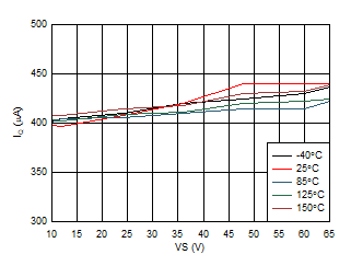
GUID-33569AA5-1DDA-4D01-A1F5-C3BFCF5B8059-low.gifFigure 6-2 Operating Quiescent Current vs Supply Voltage (> 10 V)
Figure 6-4 Charge Pump Current vs Supply Voltage at CAP = 6 V
Figure 6-6 DGATE Drive Voltage vs Supply Voltage
Figure 6-8 ANODE Leakage Current vs Reverse ANODE Voltage
Figure 6-10 OVP Thresholds vs Temperature
Figure 6-12 VA POR Threshold vs Temperature
Figure 6-14 HGATE Turn OFF Delay During OV