SNVSAU3B December 2017 – October 2019 LM76002-Q1 , LM76003-Q1
PRODUCTION DATA.
- 1 Features
- 2 Applications
- 3 Description
- 4 Revision History
- 5 Pin Configuration and Functions
- 6 Specifications
-
7 Detailed Description
- 7.1 Overview
- 7.2 Functional Block Diagram
- 7.3
Feature Description
- 7.3.1 Fixed-Frequency, Peak-Current-Mode Control
- 7.3.2 Light Load Operation Modes — PFM and FPWM
- 7.3.3 Adjustable Output Voltage
- 7.3.4 Enable (EN Pin) and UVLO
- 7.3.5 Internal LDO, VCC UVLO, and Bias Input
- 7.3.6 Soft Start and Voltage Tracking (SS/TRK)
- 7.3.7 Adjustable Switching Frequency (RT) and Frequency Synchronization
- 7.3.8 Minimum On-Time, Minimum Off-Time, and Frequency Foldback at Dropout Conditions
- 7.3.9 Internal Compensation and CFF
- 7.3.10 Bootstrap Voltage and VBOOT UVLO (BOOT Pin)
- 7.3.11 Power Good and Overvoltage Protection (PGOOD)
- 7.3.12 Overcurrent and Short-Circuit Protection
- 7.3.13 Thermal Shutdown
- 7.4 Device Functional Modes
-
8 Application and Implementation
- 8.1 Application Information
- 8.2
Typical Applications
- 8.2.1 Design Requirements
- 8.2.2
Detailed Design Procedure
- 8.2.2.1 Custom Design With WEBENCH® Tools
- 8.2.2.2 Output Voltage Setpoint
- 8.2.2.3 Switching Frequency
- 8.2.2.4 Input Capacitors
- 8.2.2.5 Inductor Selection
- 8.2.2.6 Output Capacitor Selection
- 8.2.2.7 Feed-Forward Capacitor
- 8.2.2.8 Bootstrap Capacitors
- 8.2.2.9 VCC Capacitors
- 8.2.2.10 BIAS Capacitors
- 8.2.2.11 Soft-Start Capacitors
- 8.2.2.12 Undervoltage Lockout Setpoint
- 8.2.2.13 PGOOD
- 8.2.2.14 Synchronization
- 8.2.3 Application Curves
- 9 Power Supply Recommendations
- 10Layout
- 11Device and Documentation Support
- 12Mechanical, Packaging, and Orderable Information
Package Options
Mechanical Data (Package|Pins)
- RNP|30
Thermal pad, mechanical data (Package|Pins)
- RNP|30
Orderable Information
7.3.5 Internal LDO, VCC UVLO, and Bias Input
The LM76002-Q1/LM76003-Q1 has an internal LDO generating VCC voltage for control circuitry and MOSFET drivers. The nominal voltage for VCC is 3.29 V. The VCC pin must have a 1-µF to 4.7-µF bypass capacitor placed as close as possible to the pin and properly grounded. Do not load or short the VCC pin to ground during operation. Shorting the VCC pin to ground during operation may damage the device.
An UVLO prevents the LM76002-Q1/LM76003-Q1 from operating until the VCC voltage exceeds VCC_UVLO. The VCC_UVLO threshold is 3.14 V and has approximately 575 mV of hysteresis, so the device operates until VCC drops below 2.575 V (typical). Hysteresis prevents the device from turning off during power up if VIN droops due to input current demands.
The LDO can generate VCC from two inputs: the supply voltage VIN and the BIAS input. The LDO power loss is calculated by ILDO × (VINLDO – VOUTLDO). The higher the difference between the input and output voltages of the LDO, the more losses occur to supply the same LDO output current. The BIAS input is designed to reduce the difference of the input and output voltages of the LDO to improve efficiency, especially at light load. TI recommends tying the BIAS pin to VOUT when the output voltage is equal to or greater than 3.3 V. Tie the BIAS pin to ground for applications less than 3.3 V. BIAS can also tie to external voltage source if available to improve efficiency. When used, TI recommends a 1-µF to 10-µF high-quality ceramic capacitor be used to bypass the BIAS pin to ground. If there is high-frequency noise or voltage spikes present on VOUT (during transient events or fault conditions), TI recommends connecting a resistor (1 to 10 Ω) between VOUT and BIAS.
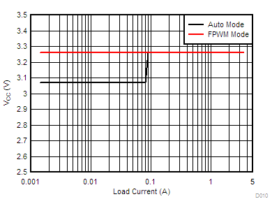
The VCC voltage is typically 3.27 V. When the LM76002-Q1/LM76003-Q1 is operating in PFM mode with frequency foldback, VCC voltage is reduced to 3.1 V (typical) to further decrease the quiescent current and improve efficiency at very light loads. Figure 13 shows an example of VCC voltage change with mode change.
 Figure 13. VCC Voltage Change With Mode Change
 VCC voltage has an internal undervoltage lockout threshold, VCC_UVLO. When VCC voltage is higher than VCC_UVLO rising threshold, the device is active and in normal operation if VEN > VEN_VOUT_H. If VCC voltage droops below VCC_UVLO falling threshold, the VOUT is shut down.