SNOSBT0L February 2000 – September 2016 LM340
PRODUCTION DATA.
- 1 Features
- 2 Applications
- 3 Description
- 4 Revision History
- 5 Pin Configuration and Functions
-
6 Specifications
- 6.1 Absolute Maximum Ratings
- 6.2 ESD Ratings
- 6.3 Recommended Operating Conditions
- 6.4 Thermal Information
- 6.5 LM340A Electrical Characteristics, VO = 5 V, VI = 10 V
- 6.6 LM340 / LM7805 Electrical Characteristics, VO = 5 V, VI = 10 V
- 6.7 LM340 / LM7812 Electrical Characteristics, VO = 12 V, VI = 19 V
- 6.8 LM340 / LM7815 Electrical Characteristics, VO = 15 V, VI = 23 V
- 6.9 Typical Characteristics
- 7 Detailed Description
- 8 Application and Implementation
- 9 Power Supply Recommendations
- 10Layout
- 11Device and Documentation Support
- 12Mechanical, Packaging, and Orderable Information
Package Options
Mechanical Data (Package|Pins)
Thermal pad, mechanical data (Package|Pins)
Orderable Information
10.3 Heat Sinking DDPAK/TO-263 and SOT-223 Package Parts
Both the DDPAK/TO-263 (KTT) and SOT-223 (DCY) packages use a copper plane on the PCB and the PCB itself as a heat sink. To optimize the heat sinking ability of the plane and PCB, solder the tab of the plane.
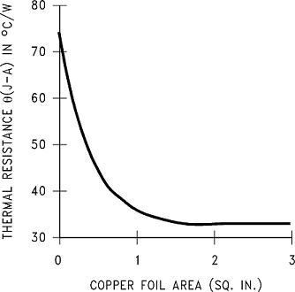
Figure 29 shows for the DDPAK/TO-263 the measured values of θ(J–A) for different copper area sizes using a typical PCB with 1-oz copper and no solder mask over the copper area used for heat sinking.
 Figure 29. θ(J–A) vs Copper (1 Ounce) Area for the DDPAK/TO-263 Package
 As shown in Figure 29, increasing the copper area beyond 1 square inch produces very little improvement. It should also be observed that the minimum value of θ(J–A) for the DDPAK/TO-263 package mounted to a PCB is 32°C/W.
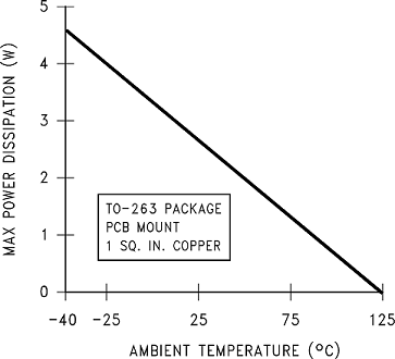
As a design aid, Figure 30 shows the maximum allowable power dissipation compared to ambient temperature for the DDPAK/TO-263 device (assuming θ(J–A) is 35°C/W and the maximum junction temperature is 125°C).
 Figure 30. Maximum Power Dissipation vs TAMB for the DDPAK/TO-263 Package
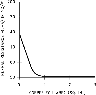
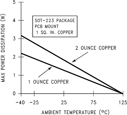
 Figure 31 and Figure 32 show the information for the SOT-223 package. Figure 31 assumes a θ(J–A) of 74°C/W for 1-oz. copper and 51°C/W for 2-oz. copper and a maximum junction temperature of 125°C.
 Figure 31. θ(J–A) vs Copper (2 Ounce) Area
for the SOT-223 Package
 Figure 32. Maximum Power Dissipation vs
TAMB for the SOT-223 Package
See AN-1028 LMX2370 PLLatinum Dual Freq Synth for RF Pers Comm LMX2370 2.5GHz/1.2GHz (SNVA036) for power enhancement techniques to be used with the SOT-223 package.