SNAS461G May   2010  – November 2018 LM98640QML-SP

PRODUCTION DATA.  

  1. Features
  2. Applications
  3. Description
  4. Revision History
  5. Pin Configuration and Functions
    1.     Pin Functions
  6. Specifications
    1. 6.1 Absolute Maximum Ratings
    2. 6.2 ESD Ratings    
    3. 6.3 Recommended Operating Conditions
    4. 6.4 Thermal Information         
    5. 6.5 Quality Conformance Inspection
    6. 6.6 LM98640QML-SP Electrical Characteristics
    7. 6.7 AC Timing Specifications
    8. 6.8 Typical Performance Characteristics
  7. Detailed Description
    1. 7.1 Overview
    2. 7.2 Functional Block Diagram
    3. 7.3 Feature Description
      1. 7.3.1 Input Sampling Modes
        1. 7.3.1.1 Sample & Hold Mode
          1. 7.3.1.1.1 Sample & Hold Mode CLAMP/SAMPLE Adjust
        2. 7.3.1.2 CDS Mode
          1. 7.3.1.2.1 CDS Mode Bimodal Offset
          2. 7.3.1.2.2 CDS Mode CLAMP/SAMPLE Adjust
      2. 7.3.2 Input Bias and Clamping
        1. 7.3.2.1 Sample and Hold Mode Biasing
        2. 7.3.2.2 CDS Mode Biasing
        3. 7.3.2.3 VCLP DAC
      3. 7.3.3 Programmable Gain
        1. 7.3.3.1 CDS/SH Stage Gain
        2. 7.3.3.2 PGA Gain Plots
      4. 7.3.4 Programmable Analog Offset Correction
      5. 7.3.5 Analog to Digital Converter
      6. 7.3.6 LVDS Output
        1. 7.3.6.1 LVDS Output Voltage
        2. 7.3.6.2 LVDS Output Modes
        3. 7.3.6.3 TXFRM Output
          1. 7.3.6.3.1 Output Mode 1 - Dual Lane
          2. 7.3.6.3.2 Output Mode 2 - Quad Lane
      7. 7.3.7 Clock Receiver
      8. 7.3.8 Power Trimming
    4. 7.4 Device Functional Mode
      1. 7.4.1 Powerdown Modes
      2. 7.4.2 LVDS Test Modes
        1. 7.4.2.1 Test Mode 0 - Fixed Pattern
        2. 7.4.2.2 Test Mode 1 - Horizontal Gradient
        3. 7.4.2.3 Test Mode 2 - Vertical Gradient
        4. 7.4.2.4 Test Mode 3 - Lattice Pattern
        5. 7.4.2.5 Test Mode 4 - Stripe Pattern
        6. 7.4.2.6 Test Mode 5 - LVDS Test Pattern (Synchronous)
        7. 7.4.2.7 Test Mode 6 - LVDS Test Pattern (Asynchronous)
        8. 7.4.2.8 Pseudo Random Number Mode
    5. 7.5 Programming
      1. 7.5.1 Serial Interface
      2. 7.5.2 Writing to the Serial Registers
      3. 7.5.3 Reading the Serial Registers
      4. 7.5.4 Serial Interface Timing Details
    6. 7.6 Register Maps
      1. 7.6.1 Register Definitions
  8. Application and Implementation
    1. 8.1 Application Information
      1. 8.1.1 Total Ionizing Dose
      2. 8.1.2 Single Event Latch-Up and Functional Interrupt
      3. 8.1.3 Single Event Effects
    2. 8.2 Typical Application
      1. 8.2.1 Sample/Hold Mode
    3. 8.3 Initialization Set Up
  9. Layout
    1. 9.1 Layout Guidelines
      1. 9.1.1 Power Planes
      2. 9.1.2 Bypass Capacitors
      3. 9.1.3 Ground Plane
      4. 9.1.4 Thermal Management
  10. 10Device and Documentation Support
    1. 10.1 Device Support
      1. 10.1.1 Development Support
        1. 10.1.1.1 Evaluation Board
        2. 10.1.1.2 Register Programming Software
    2. 10.2 Receiving Notification of Documentation Updates
    3. 10.3 Community Resources
    4. 10.4 Export Control Notice
    5. 10.5 Trademarks
    6. 10.6 Electrostatic Discharge Caution
    7. 10.7 Glossary
  11. 11Mechanical, Packaging, and Orderable Information
    1. 11.1 Engineering Samples

Package Options

Refer to the PDF data sheet for device specific package drawings

Mechanical Data (Package|Pins)
  • NBB|68
Thermal pad, mechanical data (Package|Pins)
Orderable Information

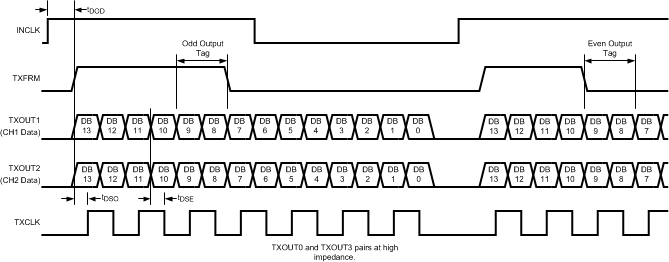
Output Mode 1 - Dual Lane

In Dual Lane mode each input channel has its own data output presented at 16x the pixel clock rate. A frame signal (TXFRM) is output at the pixel clock rate with the rising edge occurring coincident with the transition of the MSB of the data. In Sample/Hold Modes of operation, the falling edge is coincident with the transition of bit 7 of the data. In CDS Mode, the falling edge of TXFRM toggles between the transition of bit 9 and bit 7 of the data. A differential clock is also output with transitions aligned with the center of the data eye. Data rates for Dual Lane mode range from 80 Mbps, with a 5-MHz clock, up to 640 Mbps, with a 40-MHz clock.
LM98640QML-SP 30064752.gifFigure 24. Dual Lane LVDS Output Timing Diagram