SNAS461G May   2010  – November 2018 LM98640QML-SP

PRODUCTION DATA.  

  1. Features
  2. Applications
  3. Description
  4. Revision History
  5. Pin Configuration and Functions
    1.     Pin Functions
  6. Specifications
    1. 6.1 Absolute Maximum Ratings
    2. 6.2 ESD Ratings    
    3. 6.3 Recommended Operating Conditions
    4. 6.4 Thermal Information         
    5. 6.5 Quality Conformance Inspection
    6. 6.6 LM98640QML-SP Electrical Characteristics
    7. 6.7 AC Timing Specifications
    8. 6.8 Typical Performance Characteristics
  7. Detailed Description
    1. 7.1 Overview
    2. 7.2 Functional Block Diagram
    3. 7.3 Feature Description
      1. 7.3.1 Input Sampling Modes
        1. 7.3.1.1 Sample & Hold Mode
          1. 7.3.1.1.1 Sample & Hold Mode CLAMP/SAMPLE Adjust
        2. 7.3.1.2 CDS Mode
          1. 7.3.1.2.1 CDS Mode Bimodal Offset
          2. 7.3.1.2.2 CDS Mode CLAMP/SAMPLE Adjust
      2. 7.3.2 Input Bias and Clamping
        1. 7.3.2.1 Sample and Hold Mode Biasing
        2. 7.3.2.2 CDS Mode Biasing
        3. 7.3.2.3 VCLP DAC
      3. 7.3.3 Programmable Gain
        1. 7.3.3.1 CDS/SH Stage Gain
        2. 7.3.3.2 PGA Gain Plots
      4. 7.3.4 Programmable Analog Offset Correction
      5. 7.3.5 Analog to Digital Converter
      6. 7.3.6 LVDS Output
        1. 7.3.6.1 LVDS Output Voltage
        2. 7.3.6.2 LVDS Output Modes
        3. 7.3.6.3 TXFRM Output
          1. 7.3.6.3.1 Output Mode 1 - Dual Lane
          2. 7.3.6.3.2 Output Mode 2 - Quad Lane
      7. 7.3.7 Clock Receiver
      8. 7.3.8 Power Trimming
    4. 7.4 Device Functional Mode
      1. 7.4.1 Powerdown Modes
      2. 7.4.2 LVDS Test Modes
        1. 7.4.2.1 Test Mode 0 - Fixed Pattern
        2. 7.4.2.2 Test Mode 1 - Horizontal Gradient
        3. 7.4.2.3 Test Mode 2 - Vertical Gradient
        4. 7.4.2.4 Test Mode 3 - Lattice Pattern
        5. 7.4.2.5 Test Mode 4 - Stripe Pattern
        6. 7.4.2.6 Test Mode 5 - LVDS Test Pattern (Synchronous)
        7. 7.4.2.7 Test Mode 6 - LVDS Test Pattern (Asynchronous)
        8. 7.4.2.8 Pseudo Random Number Mode
    5. 7.5 Programming
      1. 7.5.1 Serial Interface
      2. 7.5.2 Writing to the Serial Registers
      3. 7.5.3 Reading the Serial Registers
      4. 7.5.4 Serial Interface Timing Details
    6. 7.6 Register Maps
      1. 7.6.1 Register Definitions
  8. Application and Implementation
    1. 8.1 Application Information
      1. 8.1.1 Total Ionizing Dose
      2. 8.1.2 Single Event Latch-Up and Functional Interrupt
      3. 8.1.3 Single Event Effects
    2. 8.2 Typical Application
      1. 8.2.1 Sample/Hold Mode
    3. 8.3 Initialization Set Up
  9. Layout
    1. 9.1 Layout Guidelines
      1. 9.1.1 Power Planes
      2. 9.1.2 Bypass Capacitors
      3. 9.1.3 Ground Plane
      4. 9.1.4 Thermal Management
  10. 10Device and Documentation Support
    1. 10.1 Device Support
      1. 10.1.1 Development Support
        1. 10.1.1.1 Evaluation Board
        2. 10.1.1.2 Register Programming Software
    2. 10.2 Receiving Notification of Documentation Updates
    3. 10.3 Community Resources
    4. 10.4 Export Control Notice
    5. 10.5 Trademarks
    6. 10.6 Electrostatic Discharge Caution
    7. 10.7 Glossary
  11. 11Mechanical, Packaging, and Orderable Information
    1. 11.1 Engineering Samples

Package Options

Refer to the PDF data sheet for device specific package drawings

Mechanical Data (Package|Pins)
  • NBB|68
Thermal pad, mechanical data (Package|Pins)
Orderable Information

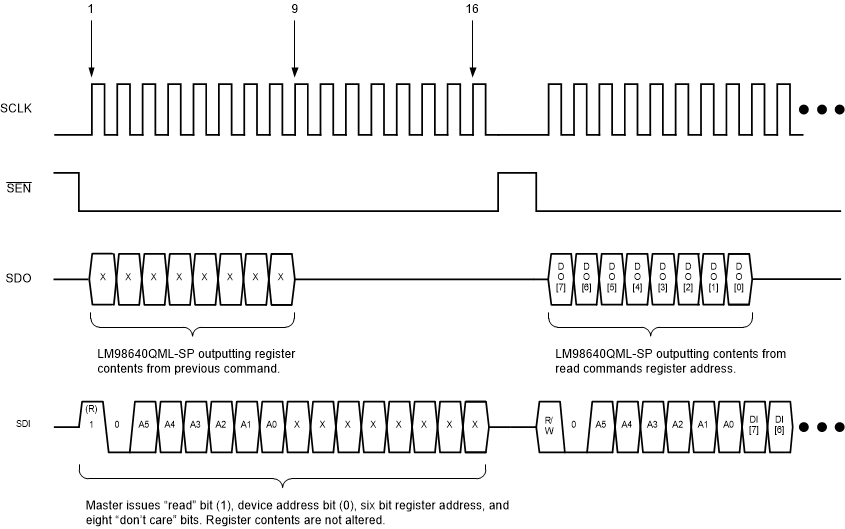
Reading the Serial Registers

To read to the serial registers using the four wire interface, the timing diagram shown in Figure 27 must be met. Reading the registers takes two cycles. To start the first cycle, SEN is toggled low. At the rising edge of the first clock, the master should assume control of the SDI pin and begin issuing the read command. The read command is built of a "read" bit (1), device address bit (0), six bit register address, and eight "don't care" bits. SDI is clocked into the LM98640QML-SP at the rising edge of SCLK. SEN is toggled high for a delay of at least tSENW (see Figure 28). The second cycle begins when SEN is toggled low. The LM98640QML-SP assumes control of the SDO pin during the first eight clocks of the cycle. During this period, data is clocked out of the device at the rising edge of SCLK. The eight bit value clocked out is the contents of the previously addressed register. The next command can be sent on the SDI pin simultaneously during this second cycle. When SEN toggles high, the register is not written to, but its contents are staged to be outputted at the beginning of the next command.
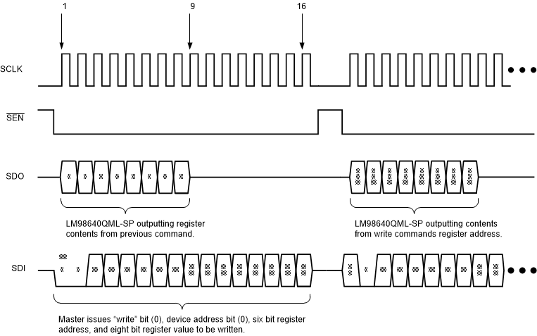
LM98640QML-SP 30064759.gifFigure 26. Four Wire Serial Write
LM98640QML-SP 30064760.gifFigure 27. Four Wire Serial Read