SNOS719G September 1999 – September 2015 LMC7101 , LMC7101Q-Q1
PRODUCTION DATA.
- 1 Features
- 2 Applications
- 3 Description
- 4 Revision History
- 5 Pin Configuration and Functions
-
6 Specifications
- 6.1 Absolute Maximum Ratings
- 6.2 ESD Ratings: LMC7101
- 6.3 ESD Ratings: LMC7101Q-Q1
- 6.4 Recommended Operating Conditions
- 6.5 Thermal Information
- 6.6 Electrical Characteristics: 2.7 V
- 6.7 DC Electrical Characteristics: 3 V
- 6.8 DC Electrical Characteristics: 5 V
- 6.9 DC Electrical Characteristics: 15 V
- 6.10 AC Electrical Characteristics: 5 V
- 6.11 AC Electrical Characteristics: 15 V
- 6.12 Typical Characteristics
- 7 Detailed Description
- 8 Application and Implementation
- 9 Power Supply Recommendations
- 10Layout
- 11Device and Documentation Support
- 12Mechanical, Packaging, and Orderable Information
Package Options
Mechanical Data (Package|Pins)
- DBV|5
Thermal pad, mechanical data (Package|Pins)
Orderable Information
7 Detailed Description
7.1 Overview
The LMC7101 is a single channel, low-power operational amplifier available in a space-saving SOT-23 package, offering rail-to-rail input and output operation across a wide range of power supply configurations. The LMC7101Q-Q1 is the automotive Q-grade variant.
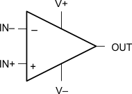
7.2 Functional Block Diagram

7.3 Feature Description
7.3.1 Benefits of the LMC7101 Tiny Amplifier
7.3.1.1 Size
The small footprint of the SOT-23-5 packaged tiny amplifier, (0.12 × 0.118 inches, 3.05 × 3 mm) saves space on printed circuit boards, and enable the design of smaller electronic products. Because they are easier to carry, many customers prefer smaller and lighter products.
7.3.1.2 Height
The 0.056 inches (1.43 mm) height of the tiny amplifier makes is suitable for use in a wide range of portable applications in which a thin profile is required.
7.3.1.3 Signal Integrity
Signals can pick up noise between the signal source and the amplifier. By using a physically smaller amplifier package, the tiny amplifier can be placed closer to the signal source, thus reducing noise pickup and increasing signal integrity. The tiny amplifier can also be placed next to the signal destination, such as a buffer, for the reference of an analog-to-digital converter.
7.3.1.4 Simplified Board Layout
The tiny amplifier can simplify board layout in several ways. Avoid long PCB traces by correctly placing amplifiers instead of routing signals to a dual or quad device.
By using multiple tiny amplifiers instead of duals or quads, complex signal routing and possibly crosstalk can be reduced.
7.3.1.5 Low THD
The high open-loop gain of the LMC7101 amp allows it to achieve very low audio distortion—typically 0.01% at 10 kHz with a 10-kΩ load at 5-V supplies. This makes the tiny amplifier an excellent for audio, modems, and low frequency signal processing.
7.3.1.6 Low Supply Current
The typical 0.5-mA supply current of the LMC7101 extends battery life in portable applications, and may allow the reduction of the size of batteries in some applications.
7.3.1.7 Wide Voltage Range
The LMC7101 is characterized at 15 V, 5 V and 3 V. Performance data is provided at these popular voltages. This wide voltage range makes the LMC7101 a good choice for devices where the voltage may vary over the life of the batteries.
7.4 Device Functional Modes
7.4.1 Input Common Mode
7.4.1.1 Voltage Range
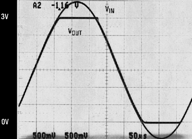
The LMC7101 does not exhibit phase inversion when an input voltage exceeds the negative supply voltage. Figure 61 shows an input voltage exceeding both supplies with no resulting phase inversion of the output.
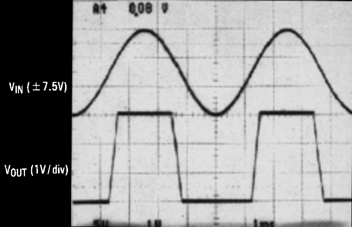
The absolute maximum input voltage is 300-mV beyond either rail at room temperature. Voltages greatly exceeding this maximum rating, as in Figure 62, can cause excessive current to flow in or out of the input pins, thus adversely affecting reliability.

NOTE:
An input voltage signal exceeds the LMC7101 power supply voltages with no output phase inversion.
NOTE:
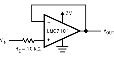
A ±7.5-V input signal greatly exceeds the 3-V supply in Figure 63 causing no phase inversion due to RI.Applications that exceed this rating must externally limit the maximum input current to ±5 mA with an input resistor as shown in Figure 63.
 Figure 63. RI Input Current Protection for
Voltages Exceeding the Supply Voltage