SNOS719G September 1999 – September 2015 LMC7101 , LMC7101Q-Q1
PRODUCTION DATA.
- 1 Features
- 2 Applications
- 3 Description
- 4 Revision History
- 5 Pin Configuration and Functions
-
6 Specifications
- 6.1 Absolute Maximum Ratings
- 6.2 ESD Ratings: LMC7101
- 6.3 ESD Ratings: LMC7101Q-Q1
- 6.4 Recommended Operating Conditions
- 6.5 Thermal Information
- 6.6 Electrical Characteristics: 2.7 V
- 6.7 DC Electrical Characteristics: 3 V
- 6.8 DC Electrical Characteristics: 5 V
- 6.9 DC Electrical Characteristics: 15 V
- 6.10 AC Electrical Characteristics: 5 V
- 6.11 AC Electrical Characteristics: 15 V
- 6.12 Typical Characteristics
- 7 Detailed Description
- 8 Application and Implementation
- 9 Power Supply Recommendations
- 10Layout
- 11Device and Documentation Support
- 12Mechanical, Packaging, and Orderable Information
Package Options
Mechanical Data (Package|Pins)
- DBV|5
Thermal pad, mechanical data (Package|Pins)
Orderable Information
6 Specifications
6.1 Absolute Maximum Ratings
over operating free-air temperature range (unless otherwise noted)(1)(4)| MIN | MAX | UNIT | |
|---|---|---|---|
| Difference input voltage | ±Supply Voltage | ||
| Voltage at input and output pins | (V+) + 0.3, (V–) – 0.3 | V | |
| Supply voltage (V+ – V–) | 16 | V | |
| Current at input pin | –5 | 5 | mA |
| Current at output pin(2) | –35 | 35 | mA |
| Current at power supply pin | 35 | mA | |
| Lead temperature (soldering, 10 sec.) | 260 | °C | |
| Junction temperature(3) | 150 | °C | |
| Storage temperature | –65 | 150 | °C |
(1) Stresses beyond those listed under Absolute Maximum Ratings may cause permanent damage to the device. These are stress ratings only, which do not imply functional operation of the device at these or any other conditions beyond those indicated under Recommended Operating Conditions. Exposure to absolute-maximum-rated conditions for extended periods may affect device reliability.
(2) Applies to both single-supply and split-supply operation. Continuous short operation at elevated ambient temperature can result in exceeding the maximum allowed junction temperature at 150°C.
(3) The maximum power dissipation is a function of TJ(MAX), RθJA and TA. The maximum allowable power dissipation at any ambient temperature is PD = (TJ(MAX) – TA) / RθJA. All numbers apply for packages soldered directly into a PC board.
(4) If Military/Aerospace specified devices are required, contact the TI Sales Office or Distributors for availability and specifications.
6.2 ESD Ratings: LMC7101
| VALUE | UNIT | |||
|---|---|---|---|---|
| V(ESD) | Electrostatic discharge | Human body model (HBM), per ANSI/ESDA/JEDEC JS-001(1) | ±1000 | V |
| Charged-device model (CDM), per JEDEC specification JESD22-C101(2) | ±1000 | |||
| Machine model (MM) | ±200 | |||
(1) JEDEC document JEP155 states that 500-V HBM allows safe manufacturing with a standard ESD control process.
(2) JEDEC document JEP157 states that 250-V CDM allows safe manufacturing with a standard ESD control process.
6.3 ESD Ratings: LMC7101Q-Q1
| VALUE | UNIT | |||
|---|---|---|---|---|
| V(ESD) | Electrostatic discharge | Human body model (HBM), per ANSI/ESDA/JEDEC JS-001(1) | ±1000 | V |
| Charged-device model (CDM), per JEDEC specification JESD22-C101 | ±1000 | |||
| Machine model (MM) | ±200 | |||
(1) AEC Q100-002 indicates that HBM stressing shall be in accordance with the ANSI/ESDA/JEDEC JS-001 specification.
6.4 Recommended Operating Conditions
over operating free-air temperature range (unless otherwise noted).(1)| MIN | MAX | UNIT | ||
|---|---|---|---|---|
| Supply voltage, V+ | 2.7 | 15.5 | V | |
| Junction Temperature, TJ | LMC7101AI, LMC7101BI | –40 | 85 | °C |
| LMC7101Q-Q1 | –40 | 125 | °C | |
(1) Stresses beyond those listed under Absolute Maximum Ratings may cause permanent damage to the device. These are stress ratings only, which do not imply functional operation of the device at these or any other conditions beyond those indicated under Recommended Operating Conditions. Exposure to absolute-maximum-rated conditions for extended periods may affect device reliability.
6.5 Thermal Information
| THERMAL METRIC(1) | LMC7101 | UNIT | |
|---|---|---|---|
| DBV (SOT-23) | |||
| 5 PINS | |||
| RθJA | Junction-to-ambient thermal resistance | 170.9 | °C/W |
| RθJC(top) | Junction-to-case (top) thermal resistance | 124.7 | °C/W |
| RθJB | Junction-to-board thermal resistance | 30.8 | °C/W |
| ψJT | Junction-to-top characterization parameter | 17.7 | °C/W |
| ψJB | Junction-to-board characterization parameter | 30.2 | °C/W |
| RθJC(bot) | Junction-to-case (bottom) thermal resistance | n/a | °C/W |
(1) For more information about traditional and new thermal metrics, see the Semiconductor and IC Package Thermal Metrics application report, SPRA953.
6.6 Electrical Characteristics: 2.7 V
Unless otherwise specified, all limits specified for TJ = 25°C, V+ = 2.7 V, V– = 0 V, VCM = VO = V+ / 2 and RL > 1 MΩ.| PARAMETER | TEST CONDITIONS | TYP(1) | LMC7101AI | LMC7101BI | LMC7101Q-Q1(2) | UNIT | ||||
|---|---|---|---|---|---|---|---|---|---|---|
| MIN | MAX | MIN | MAX | MIN | MAX | |||||
| VOS | Input offset voltage average drift | V+ = 2.7 V | 0.11 | 6 | 9 | 9 | mV | |||
| TCVOS | Input offset voltage | 1 | μV/°C | |||||||
| IB | Input bias current | –40°C ≤ TJ ≤ 125°C | 1 | 64 | 64 | 1000 | pA | |||
| IOS | Input offset current | –40°C ≤ TJ ≤ 125°C | 0.5 | 32 | 32 | 2000 | pA | |||
| RIN | Input resistance | >1 | Tera Ω | |||||||
| CMRR | Common-mode rejection ratio | 0 V ≤ VCM ≤ 2.7 V V+ = 2.7 V |
70 | 55 | 50 | 50 | dB | |||
| VCM | Input common mode voltage range | For CMRR ≥ 50 dB | 0 | 0 | 0 | 0 | V | |||
| 3 | 2.7 | 2.7 | 2.7 | V | ||||||
| PSRR | Power supply rejection ratio | V+ = 1.35 V to 1.65 V V– = –1.35 V to –1.65 V VCM = 0 |
60 | 50 | 45 | 45 | dB | |||
| CIN | Common-mode input capacitance | 3 | pF | |||||||
| VO | Output swing, min | RL = 2 kΩ | 2.45 | 2.15 | 2.15 | 2.15 | V | |||
| RL = 10 kΩ | 2.68 | 2.64 | 2.64 | 2.64 | ||||||
| VO | Output swing, max | RL = 2 kΩ | 0.25 | 0.5 | 0.5 | 0.5 | V | |||
| RL = 10 kΩ | 0.025 | 0.06 | 0.06 | 0.06 | ||||||
| IS | Supply current | 0.5 | 0.81 | 0.81 | 0.81 | mA | ||||
| –40°C ≤ TJ ≤ 125°C | 0.5 | 0.95 | 0.95 | 0.95 | ||||||
| SR | Slew rate(3) | 0.7 | V/μs | |||||||
| GBW | Gain-bandwidth product | 0.6 | MHz | |||||||
(1) Typical values represent the most likely parametric normal.
(2) When operated at temperature between –40°C and 85°C, the LMC7101Q-Q1 will meet LMC7101BI specifications.
(3) V+ = 15 V. Connected as a voltage follower with a 10-V step input. Number specified is the slower of the positive and negative slew rates. RL = 100 kΩ connected to 7.5 V. Amplifier excited with 1 kHz to produce VO = 10 VPP.
6.7 DC Electrical Characteristics: 3 V
Unless otherwise specified, all limits specified for TJ = 25°C, V+ = 3 V, V– = 0 V, VCM = 1.5 V, VO = V+ / 2 and RL = 1 MΩ.| PARAMETER | TEST CONDITIONS | TYP(1) | LMC7101AI | LMC7101BI | LMC7101Q-Q1(2) | UNIT | ||||
|---|---|---|---|---|---|---|---|---|---|---|
| MIN | MAX | MIN | MAX | MIN | MAX | |||||
| VOS | Input offset voltage | 4 | 7 | 7 | mV | |||||
| –40°C ≤ TJ ≤ 125°C | 0.11 | 6 | 9 | |||||||
| TCVOS | Input offset voltage average drift | 1 | μV/°C | |||||||
| IB | Input current | –40°C ≤ TJ ≤ 125°C | 1 | 64 | 64 | 1000 | pA | |||
| IOS | Input offset current | –40°C ≤ TJ ≤ 125°C | 0.5 | 32 | 32 | 2000 | pA | |||
| RIN | Input resistance | >1 | Tera Ω | |||||||
| CMRR | Common-mode rejection ratio | 0 V ≤ VCM ≤ 3 V V+ = 3 V |
74 | 64 | 60 | 60 | db | |||
| VCM | Input common-mode voltage range | For CMRR ≥ 50 dB | 0 | 0 | 0 | 0 | V | |||
| 3.3 | 3 | 3 | 3 | |||||||
| PSRR | Power supply rejection ratio | V+ = 1.5 V to 7.5 V V– = –1.5 V to –7.5 V VO = VCM = 0 |
80 | 68 | 60 | 60 | dB | |||
| CIN | Common-mode input capacitance | 3 | pF | |||||||
| VO | Output swing, min | RL = 2 kΩ | 2.8 | 2.6 | 2.6 | 2.6 | V | |||
| RL = 600 Ω | 0.2 | 0.4 | 0.4 | 0.4 | ||||||
| VO | Output swing, max | RL = 2 kΩ | 2.7 | 2.5 | 2.5 | 2.5 | V | |||
| RL = 600 Ω | 0.37 | 0.6 | 0.6 | 0.6 | ||||||
| IS | Supply current | 0.81 | 0.81 | 0.81 | mA | |||||
| –40°C ≤ TJ ≤ 125°C | 0.5 | 0.95 | 0.95 | 0.95 | ||||||
(1) Typical values represent the most likely parametric normal.
(2) When operated at temperature between –40°C and 85°C, the LMC7101Q-Q1 will meet LMC7101BI specifications.
6.8 DC Electrical Characteristics: 5 V
Unless otherwise specified, all limits specified for TJ = 25°C, V+ = 5 V, V– = 0 V, VCM = 1.5 V, VO = V+/ 2 and RL = 1 MΩ.| PARAMETER | TEST CONDITIONS | TYP(1) | LMC7101AI | LMC7101BI | LMC7101Q-Q1(2) | UNIT | |||||
|---|---|---|---|---|---|---|---|---|---|---|---|
| MIN | MAX | MIN | MAX | MIN | MAX | ||||||
| VOS | Input offset voltage | V+ = 5 V | 0.11 | 3 | 7 | 7 | mV | ||||
| V+ = 5 V, –40°C ≤ TJ ≤ 125°C | 0.11 | 5 | 9 | 9 | |||||||
| TCVOS | Input offset voltage average drift | 1 | μV/°C | ||||||||
| IB | Input current | –40°C ≤ TJ ≤ 125°C | 1 | 64 | 64 | 1000 | pA | ||||
| IOS | Input offset current | –40°C ≤ TJ ≤ 125°C | 0.5 | 32 | 32 | 2000 | pA | ||||
| RIN | Input resistance | >1 | Tera Ω | ||||||||
| CMRR | Common-mode rejection ratio | 0 V ≤ VCM ≤ 5 V LMC7101Q-Q1 at 125°C 0.2 V ≤ VCM ≤ 4.8 V |
82 | 65 | 60 | 60 | db | ||||
| 0 V ≤ VCM ≤ 5 V LMC7101Q-Q1 at 125°C 0.2 V ≤ VCM ≤ 4.8 V –40°C ≤ TJ ≤ 125°C |
82 | 60 | 55 | 55 | |||||||
| +PSRR | Positive power supply rejection ratio | V+ = 5 V to 15 V V– = 0 V, VO = 1.5 V |
82 | 70 | 65 | 65 | dB | ||||
| V+ = 5 V to 15 V V– = 0 V, VO = 1.5 V –40°C ≤ TJ ≤ 125°C |
82 | 65 | 62 | 62 | |||||||
| –PSRR | Negative power supply rejection ratio | V– = –5 V to –15 V V+ = 0 V, VO = –1.5 V |
82 | 70 | 65 | 65 | dB | ||||
| V– = –5 V to –15 V V+ = 0 V, VO = –1.5 V –40°C ≤ TJ ≤ 125°C |
82 | 65 | 62 | 62 | |||||||
| VCM | Input common-mode voltage range | For CMRR ≥ 50 dB | –0.3 | –0.2 | –0.2 | –0.2 | V | ||||
| For CMRR ≥ 50 dB –40°C ≤ TJ ≤ 125°C |
–0.3 | 0 | 0 | 0.2 | |||||||
| 5.3 | 5.2 | 5.2 | 5.2 | V | |||||||
| –40°C ≤ TJ ≤ 125°C | 5.3 | 5 | 5 | 4.8 | |||||||
| CIN | Common-mode input capacitance | 3 | pF | ||||||||
| VO | Output swing | RL = 2 kΩ | 4.9 | 4.7 | 4.7 | 4.7 | V | ||||
| RL = 2 kΩ, –40°C ≤ TJ ≤ 125°C | 4.9 | 4.6 | 4.6 | 4.54 | |||||||
| 0.1 | 0.18 | 0.18 | 0.18 | V | |||||||
| –40°C ≤ TJ ≤ 125°C | 0.1 | 0.24 | 0.24 | 0.28 | |||||||
| RL = 600 Ω | 4.7 | 4.5 | 4.5 | 4.5 | V | ||||||
| RL = 600 Ω, –40°C ≤ TJ ≤ 125°C | 4.7 | 4.24 | 4.24 | 4.28 | |||||||
| 0.3 | 0.5 | 0.5 | 0.5 | V | |||||||
| –40°C ≤ TJ ≤ 125°C | 0.3 | 0.65 | 0.65 | 0.8 | |||||||
| ISC | Output short circuit current | Sourcing | VO = 0 V 24 | 24 | 16 | 16 | 16 | mA | |||
| VO = 0 V 24 –40°C ≤ TJ ≤ 125°C |
24 | 11 | 11 | 9 | |||||||
| Sinking | VO = 5 V | 19 | 11 | 11 | 11 | mA | |||||
| VO = 5 V –40°C ≤ TJ ≤ 125°C |
19 | 7.5 | 7.5 | 5.8 | |||||||
| IS | Supply current | 0.5 | 0.85 | 0.85 | 0.85 | mA | |||||
| –40°C ≤ TJ ≤ 125°C | 0.5 | 1 | 1 | 1 | |||||||
(1) Typical values represent the most likely parametric normal.
(2) When operated at temperature between –40°C and 85°C, the LMC7101Q-Q1 will meet LMC7101BI specifications.
6.9 DC Electrical Characteristics: 15 V
Unless otherwise specified, all limits specified for TJ = 25°C, V+ = 15 V, V– = 0 V, VCM = 1.5 V, VO = V+ / 2 and RL = 1 MΩ.| PARAMETER | TEST CONDITIONS | TYP(1) | LMC7101AI | LMC7101BI | LMC7101Q-Q1(2) | UNIT | |||||
|---|---|---|---|---|---|---|---|---|---|---|---|
| MIN | MAX | MIN | MAX | MIN | MAX | ||||||
| VOS | Input offset voltage | 0.11 | mV | ||||||||
| TCVOS | Input offset voltage average drift | 1 | μV/°C | ||||||||
| IB | Input current | –40°C ≤ TJ ≤ 125°C | 1 | 64 | 64 | 1000 | pA | ||||
| IOS | Input offset current | –40°C ≤ TJ ≤ 125°C | 0.5 | 32 | 32 | 2000 | pA | ||||
| RIN | Input resistance | >1 | Tera Ω | ||||||||
| CMRR | Common-mode rejection ratio | 0 V ≤ VCM ≤ 15 V LMC7101Q-Q1 at 125°C 0.2 V ≤ VCM ≤ 14.8 V |
82 | 70 | 65 | 65 | dB | ||||
| 0 V ≤ VCM ≤ 15 V LMC7101Q-Q1 at 125°C 0.2 V ≤ VCM ≤ 14.8 V –40°C ≤ TJ ≤ 125°C |
82 | 65 | 60 | 60 | |||||||
| +PSRR | Positive power supply rejection ratio | V+ = 5 V to 15 V V– = 0 V, VO = 1.5 V |
82 | 70 | 65 | 65 | dB | ||||
| V+ = 5 V to 15 V V– = 0 V, VO = 1.5 V –40°C ≤ TJ ≤ 125°C |
82 | 65 | 62 | 62 | |||||||
| –PSRR | Negative power supply rejection ratio | V– = –5 V to –15 V V+ = 0 V, VO = –1.5 V |
82 | 70 | 65 | 65 | dB | ||||
| V– = –5 V to –15 V V+ = 0 V, VO = –1.5 V –40°C ≤ TJ ≤ 125°C |
82 | 65 | 62 | 62 | |||||||
| VCM | Input common-mode voltage range | V+ = 5 V For CMRR ≥ 50 dB |
–0.3 | –0.2 | –0.2 | –0.2 | V | ||||
| V+ = 5 V For CMRR ≥ 50 dB –40°C ≤ TJ ≤ 125°C |
-0.3 | 0 | 0 | 0.2 | |||||||
| 15.3 | 15.2 | 15.2 | 15.2 | V max | |||||||
| –40°C ≤ TJ ≤ 125°C | 15.3 | 15 | 15 | 14.8 | |||||||
| AV | Large signal voltage gain(3) | Sourcing | RL = 2 kΩ | 340 | 80 | 80 | 80 | V/mV | |||
| RL = 2 kΩ –40°C ≤ TJ ≤ 125°C |
340 | 40 | 40 | 30 | |||||||
| Sinking | RL = 2 kΩ | 24 | 15 | 15 | 15 | ||||||
| RL = 2 kΩ –40°C ≤ TJ ≤ 125°C |
24 | 10 | 10 | 4 | |||||||
| Sourcing | RL = 600 Ω | 300 | 34 | 34 | 34 | V/mV | |||||
| Sinking | 15 | 6 | 6 | 6 | |||||||
| CIN | Input capacitance | 3 | pF | ||||||||
| VO | Output swing | V+ = 15 V RL = 2 kΩ |
14.7 | 14.4 | 14.4 | 14.4 | V | ||||
| V+ = 15 V RL = 2 kΩ –40°C ≤ TJ ≤ 125°C |
14.7 | 14.2 | 14.2 | 14.2 | |||||||
| 0.16 | 0.32 | 0.32 | 0.32 | V | |||||||
| –40°C ≤ TJ ≤ 125°C | 0.16 | 0.45 | 0.45 | 0.45 | |||||||
| V+ = 15 V RL = 600 Ω |
14.1 | 13.4 | 13.4 | 13.4 | V | ||||||
| V+ = 15 V RL = 600 Ω –40°C ≤ TJ ≤ 125°C |
14.1 | 13 | 13 | 12.85 | |||||||
| 0.5 | 1 | 1 | 1 | V | |||||||
| –40°C ≤ TJ ≤ 125°C | 0.5 | 1.3 | 1.3 | 1.5 | |||||||
| ISC | Output short circuit current(4) | Sourcing | VO = 0 V | 50 | 30 | 30 | 30 | mA | |||
| VO = 0 V –40°C ≤ TJ ≤ 125°C |
50 | 20 | 20 | 20 | |||||||
| Sinking | VO = 12 V | 50 | 30 | 30 | 30 | ||||||
| VO = 12 V –40°C ≤ TJ ≤ 125°C |
50 | 20 | 20 | 20 | |||||||
| IS | Supply current | 0.8 | 1.5 | 1.5 | 1.5 | mA | |||||
| –40°C ≤ TJ ≤ 125°C | 1.71 | 1.71 | 1.75 | ||||||||
(1) Typical values represent the most likely parametric normal.
(2) When operated at temperature between –40°C and 85°C, the LMC7101Q-Q1 will meet LMC7101BI specifications.
(3) V+ = 15 V, VCM = 1.5 V and RL connect to 7.5 V. For sourcing tests, 7.5 V ≤ VO ≤ 12.5 V. For sinking tests, 2.5 V ≤ VO ≤ 7.5 V.
(4) Do not short circuit output to V+ when V+ is greater than 12 V or reliability will be adversely affected.
6.10 AC Electrical Characteristics: 5 V
Unless otherwise specified, all limits specified for TJ = 25°C, V+ = 5 V, V– = 0 V, VCM = 1.5 V, VO = V+ / 2 and RL = 1 MΩ.| PARAMETER | TEST CONDITIONS | TYP(1) | LMC7101AI LIMIT(2) |
LMC7101BI LIMIT(2) |
UNIT | |
|---|---|---|---|---|---|---|
| THD | Total harmonic distortion | f = 10 kHz, AV = –2 RL = 10 kΩ, VO = 4 VPP |
0.01% | |||
| SR | Slew rate | 1 | V/μs | |||
| GBW | Gain bandwidth product | 1 | MHz | |||
(1) Typical values represent the most likely parametric normal.
(2) All limits are specified by testing or statistical analysis.
6.11 AC Electrical Characteristics: 15 V
Unless otherwise specified, all limits specified for TJ = 25°C, V+ = 15 V, V– = 0 V, VCM = 1.5 V, VO = V+ / 2 and RL = 1 MΩ.| PARAMETER | TEST CONDITIONS | TYP(1) | LMC7101AI | LMC7101BI | LMC7101Q-Q1(3) | UNIT | ||||
|---|---|---|---|---|---|---|---|---|---|---|
| MIN | MAX | MIN | MAX | MIN | MAX | |||||
| SR | Slew rate(2) | V+ = 15 V | 1.1 | 0.5 | 0.5 | 0.5 | V/μs min |
|||
| V+ = 15 V, –40°C ≤ TJ ≤ 125°C | 0.4 | 0.4 | 0.4 | |||||||
| GBW | Gain-bandwidth product | V+ = 15 V | 1.1 | MHz | ||||||
| φm | Phase margin | 45 | deg | |||||||
| Gm | Gain margin | 10 | dB | |||||||
| en | Input-referred voltage noise | f = 1 kHz, VCM = 1 V | 37 |  |
||||||
| In | Input-referred current noise | f = 1 kHz | 1.5 |  |
||||||
| THD | Total harmonic distortion | f = 10 kHz, AV = –2 RL = 10 kΩ VO = 8.5 VPP |
0.01% | |||||||
(1) Typical values represent the most likely parametric normal.
(2) V+ = 15 V. Connected as a voltage follower with a 10-V step input. Number specified is the slower of the positive and negative slew rates. RL = 100 kΩ connected to 7.5 V. Amplifier excited with 1 kHz to produce VO = 10 VPP.
(3) When operated at temperature between –40°C and 85°C, the LMC7101Q-Q1 will meet LMC7101BI specifications.
6.12 Typical Characteristics
6.12.1 Typical Characteristics: 2.7 V
V+ = 2.7 V, V– = 0 V, TA = 25°C, unless otherwise specified.
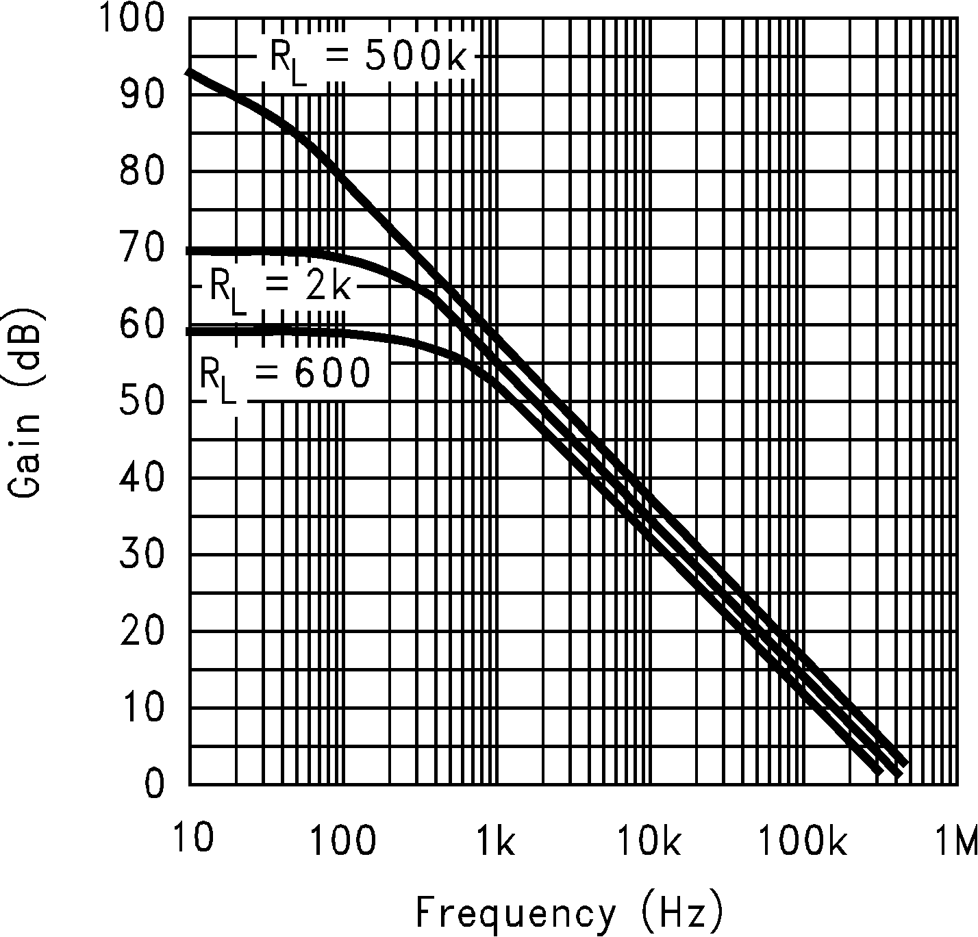 Figure 1. Open Loop Frequency Response
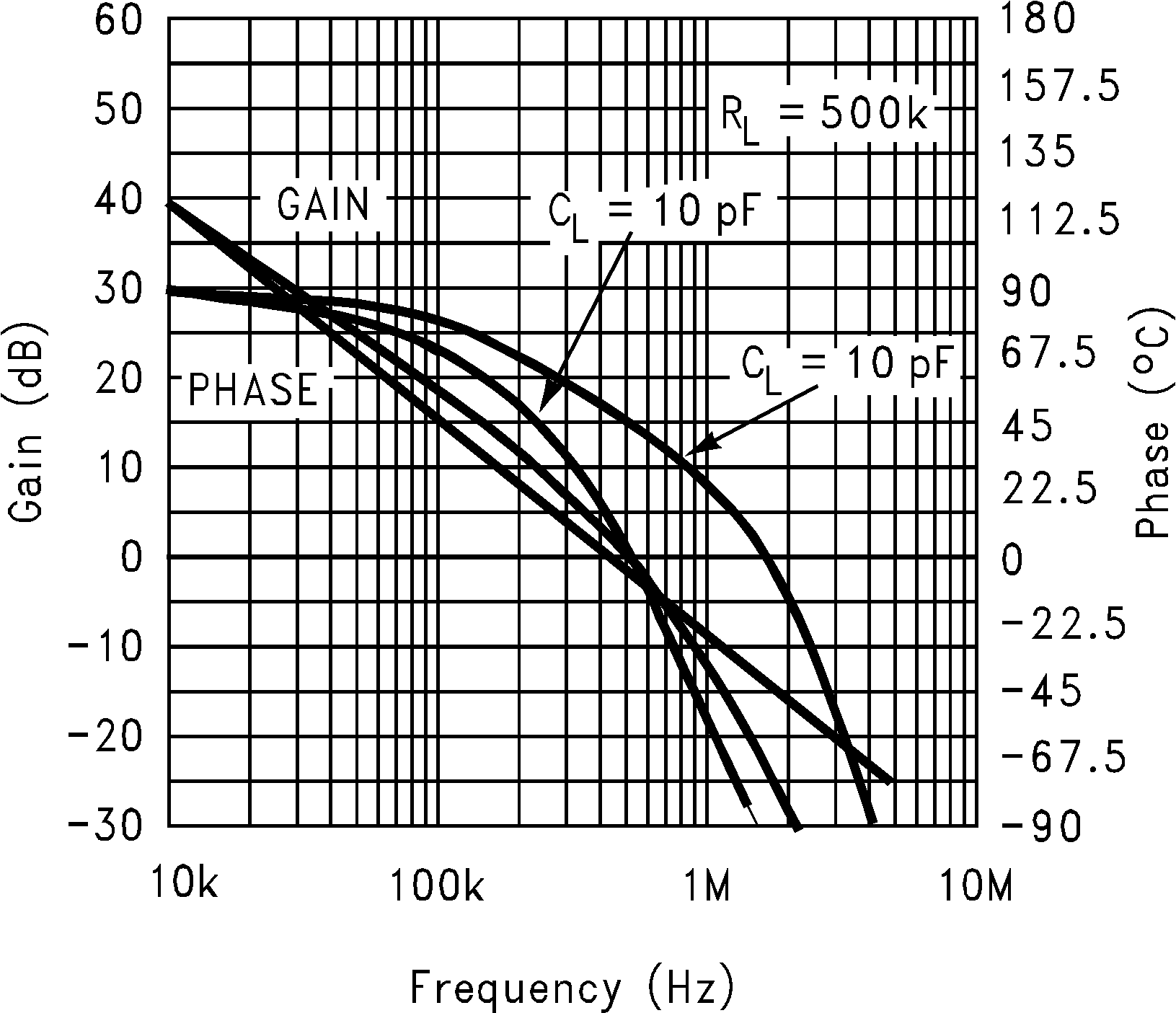 Figure 3. Gain and Phase vs Capacitance Load
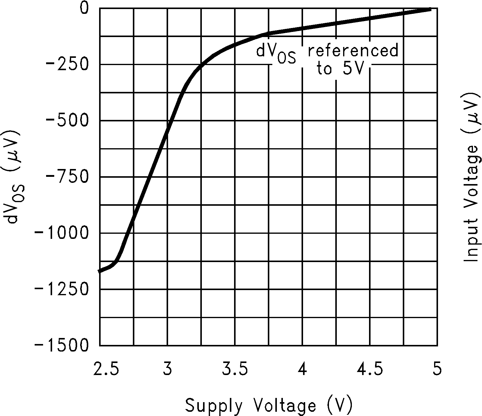 Figure 5. dVOS vs Supply Voltage
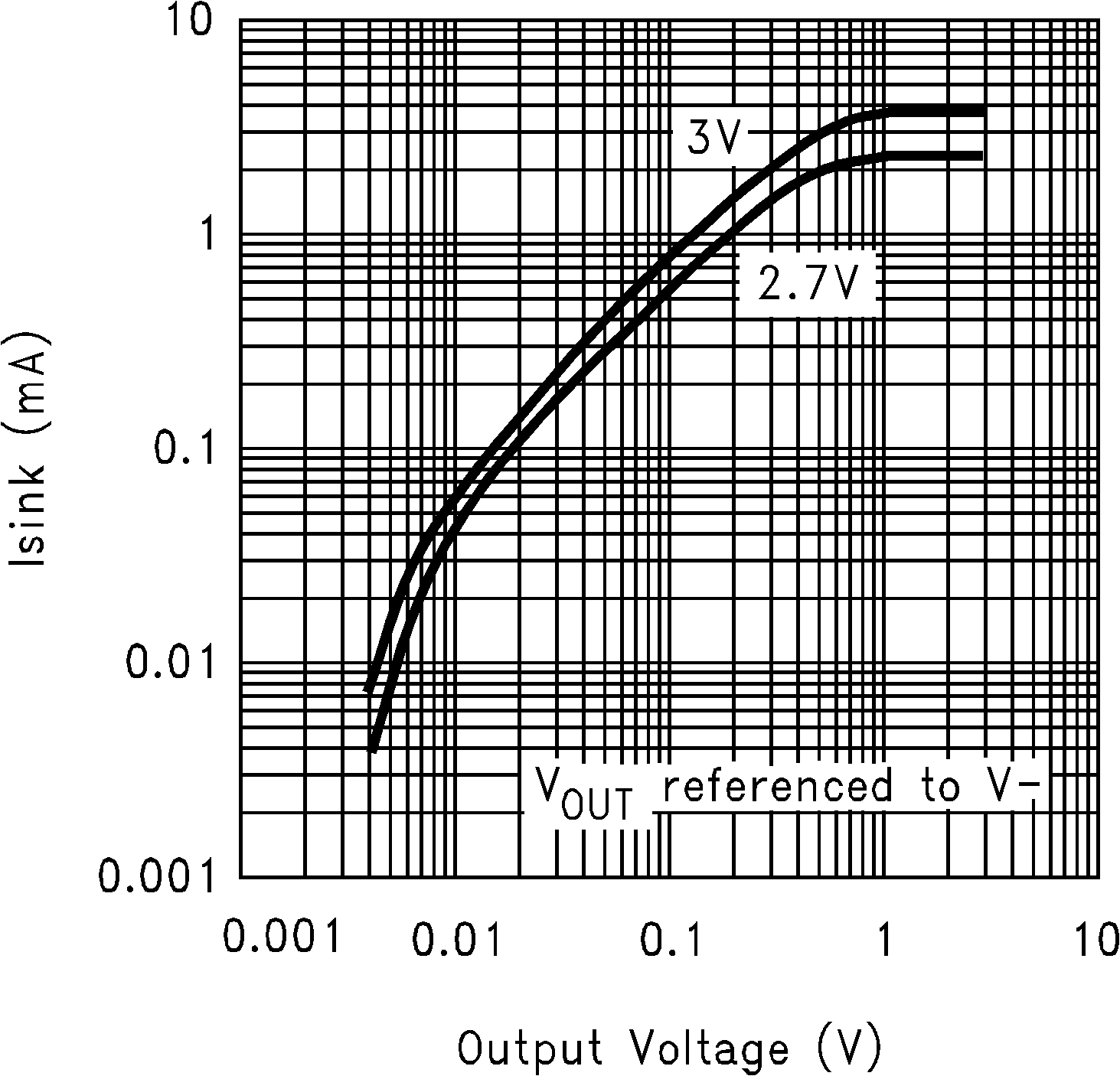 Figure 7. Sinking Current vs Output Voltage
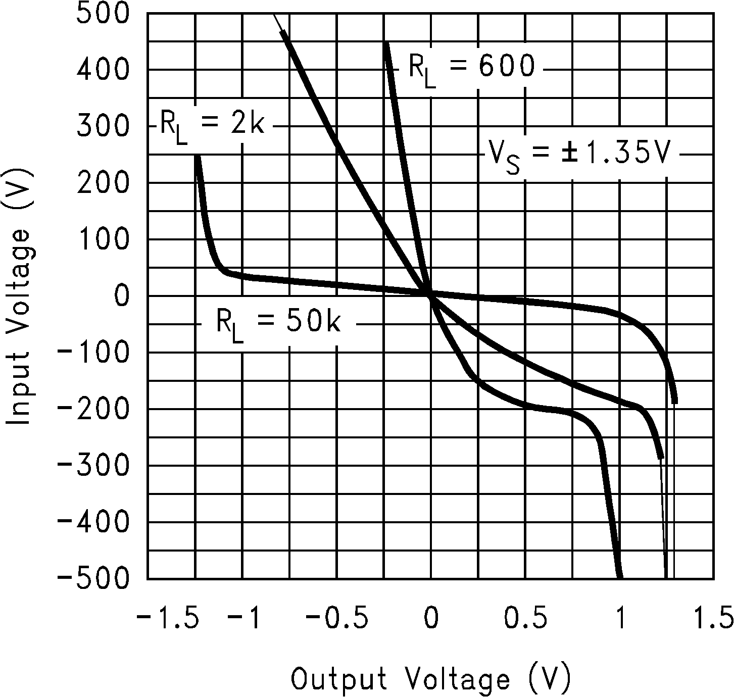 Figure 2. Input Voltage vs Output Voltage
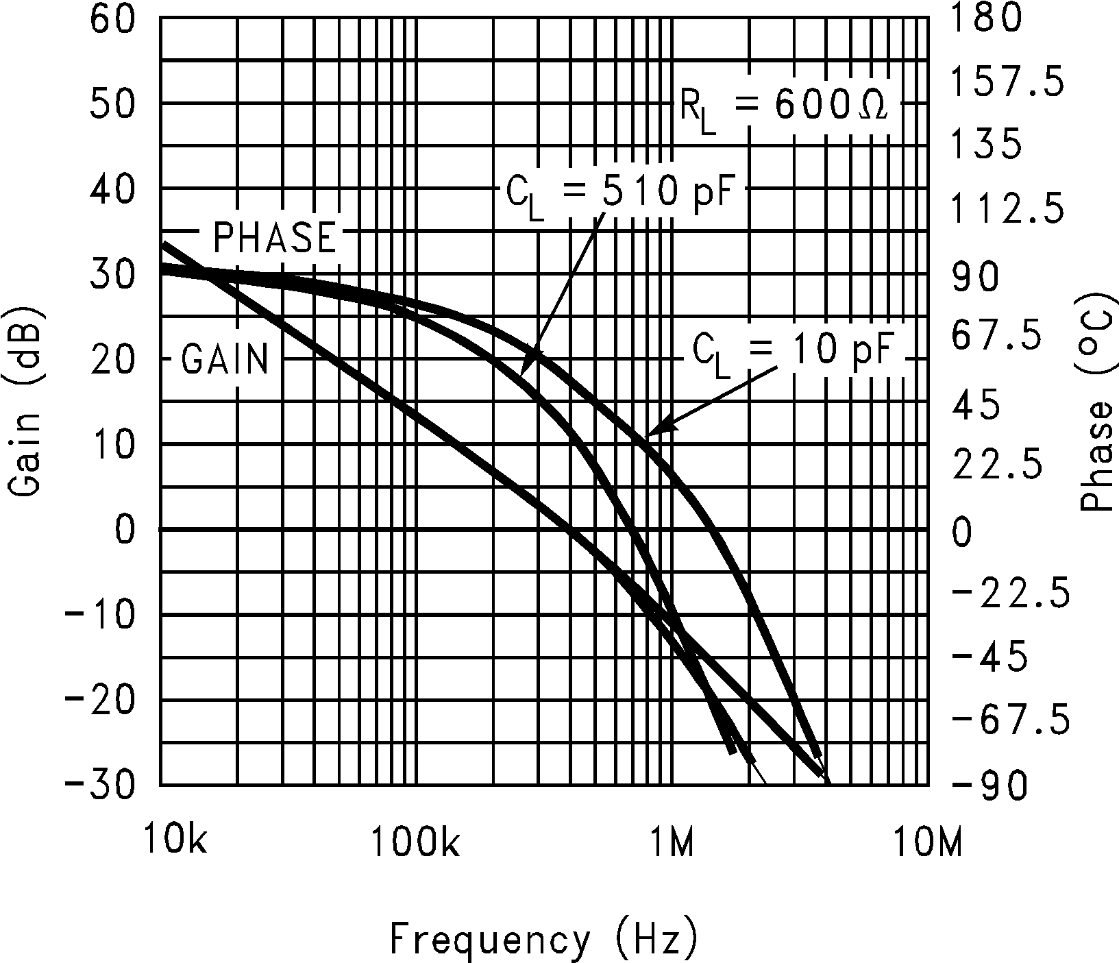 Figure 4. Gain and Phase vs Capacitance Load
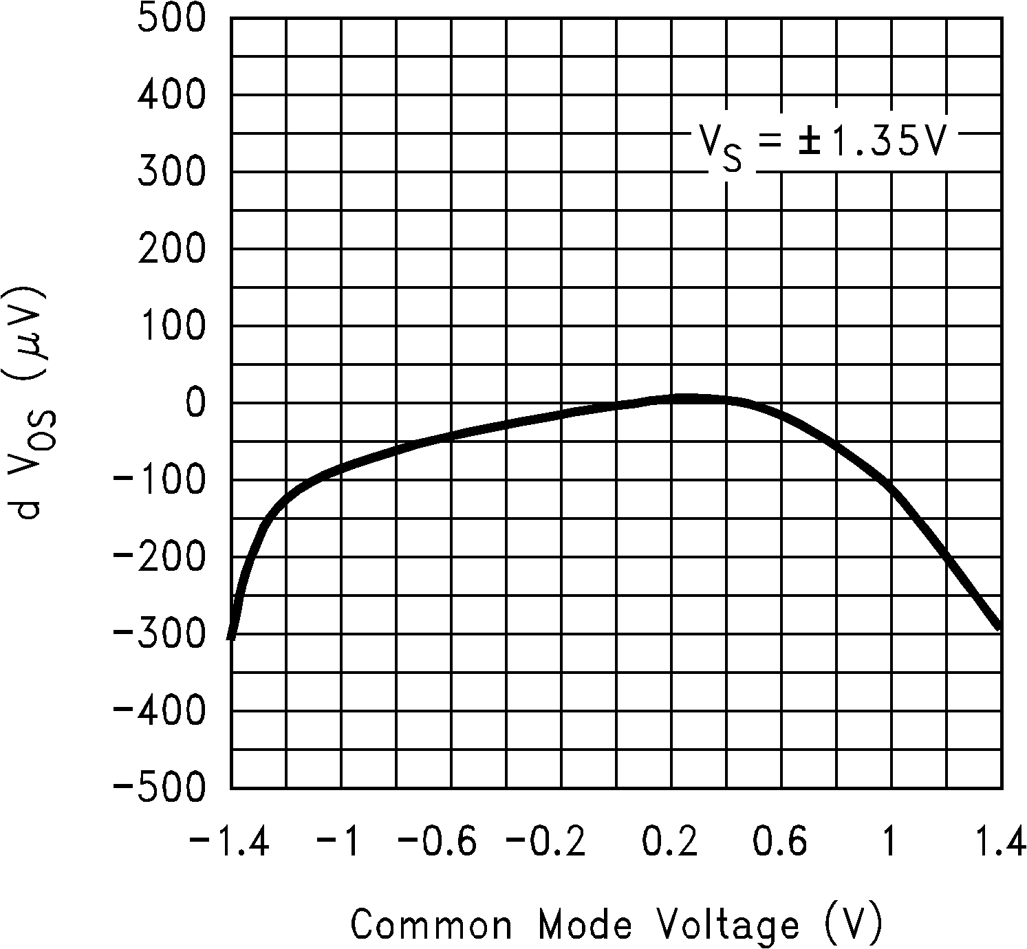 Figure 6. dVOS vs Common Mode Voltage
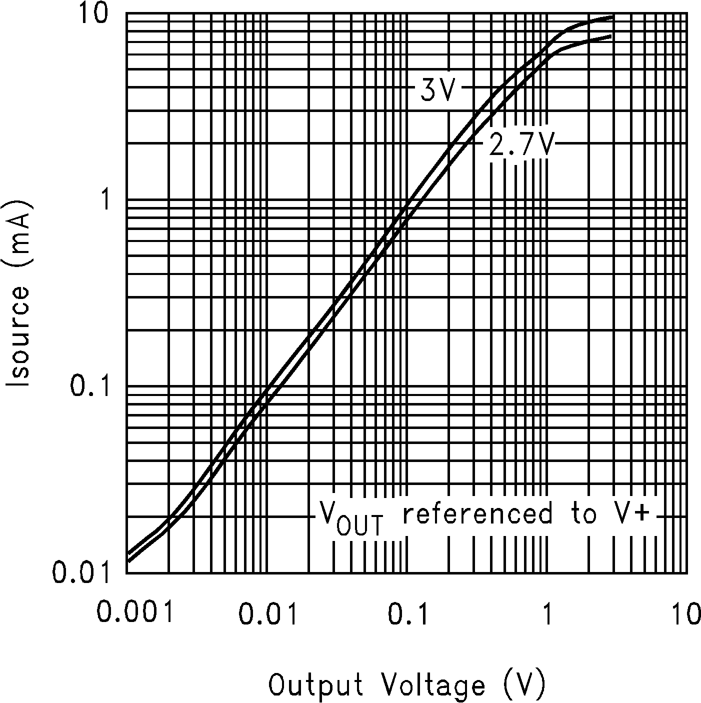 Figure 8. Sourcing Current vs Output Voltage
6.12.2 Typical Characteristics: 3 V
V+ = 3 V, V– = 0 V, TA = 25°C, unless otherwise specified.
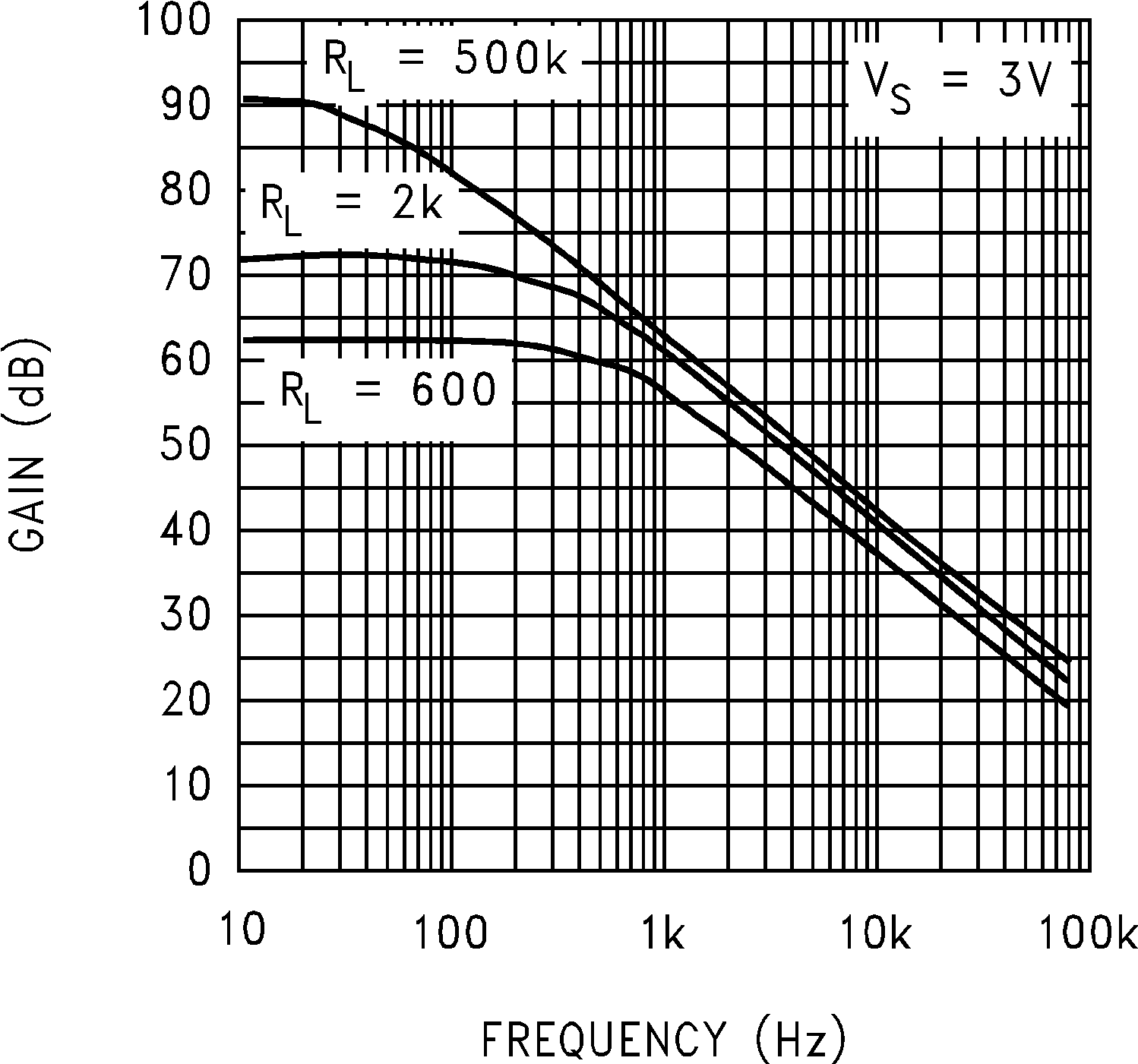 Figure 9. Open Loop Frequency Response
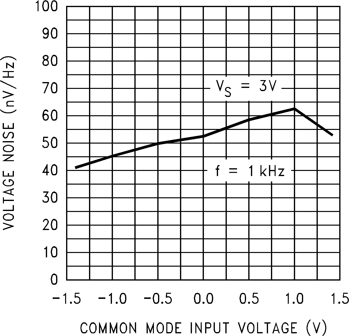 Figure 11. Input Voltage Noise vs Input Voltage
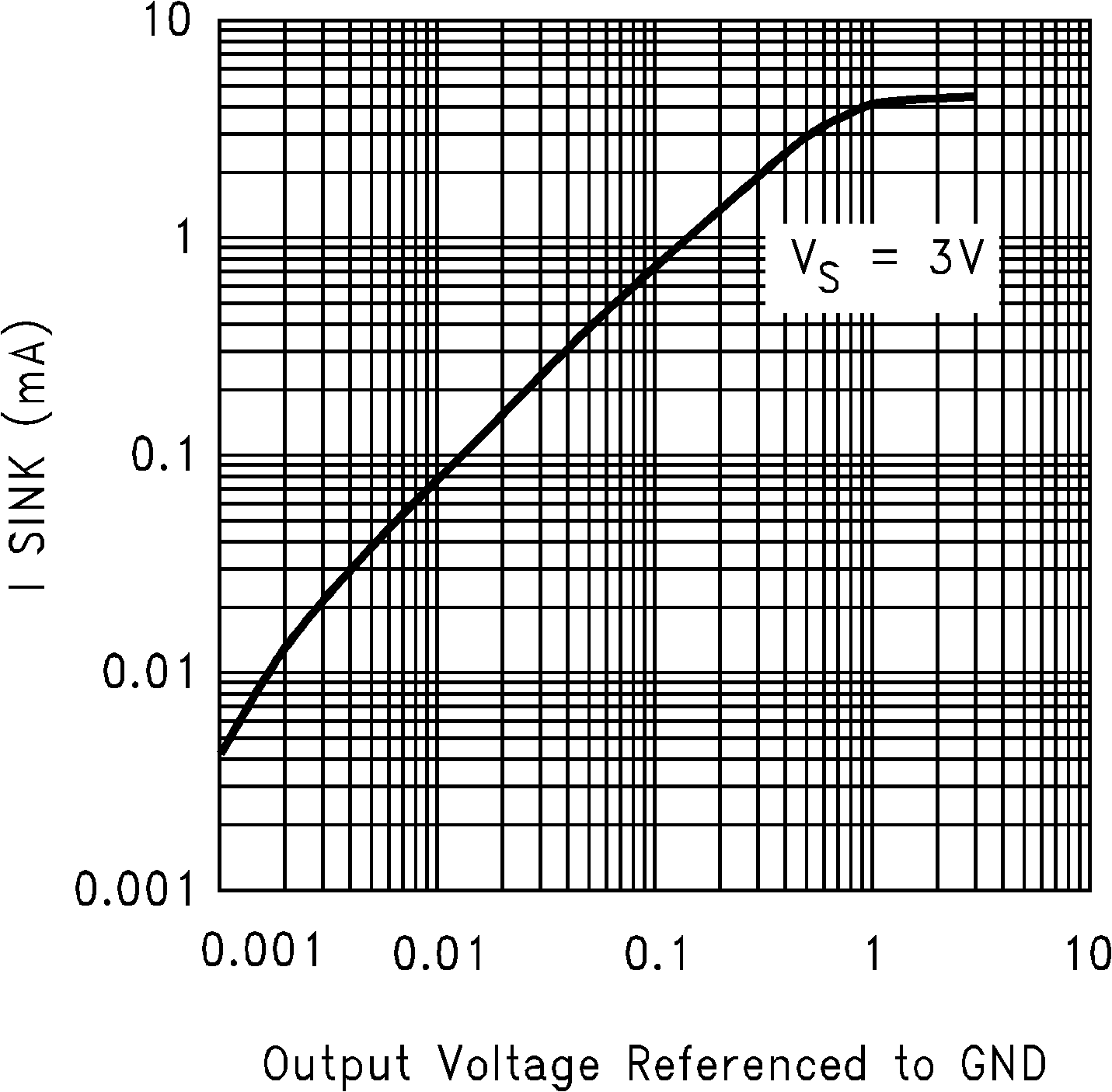 Figure 13. Sinking Current vs Output Voltage
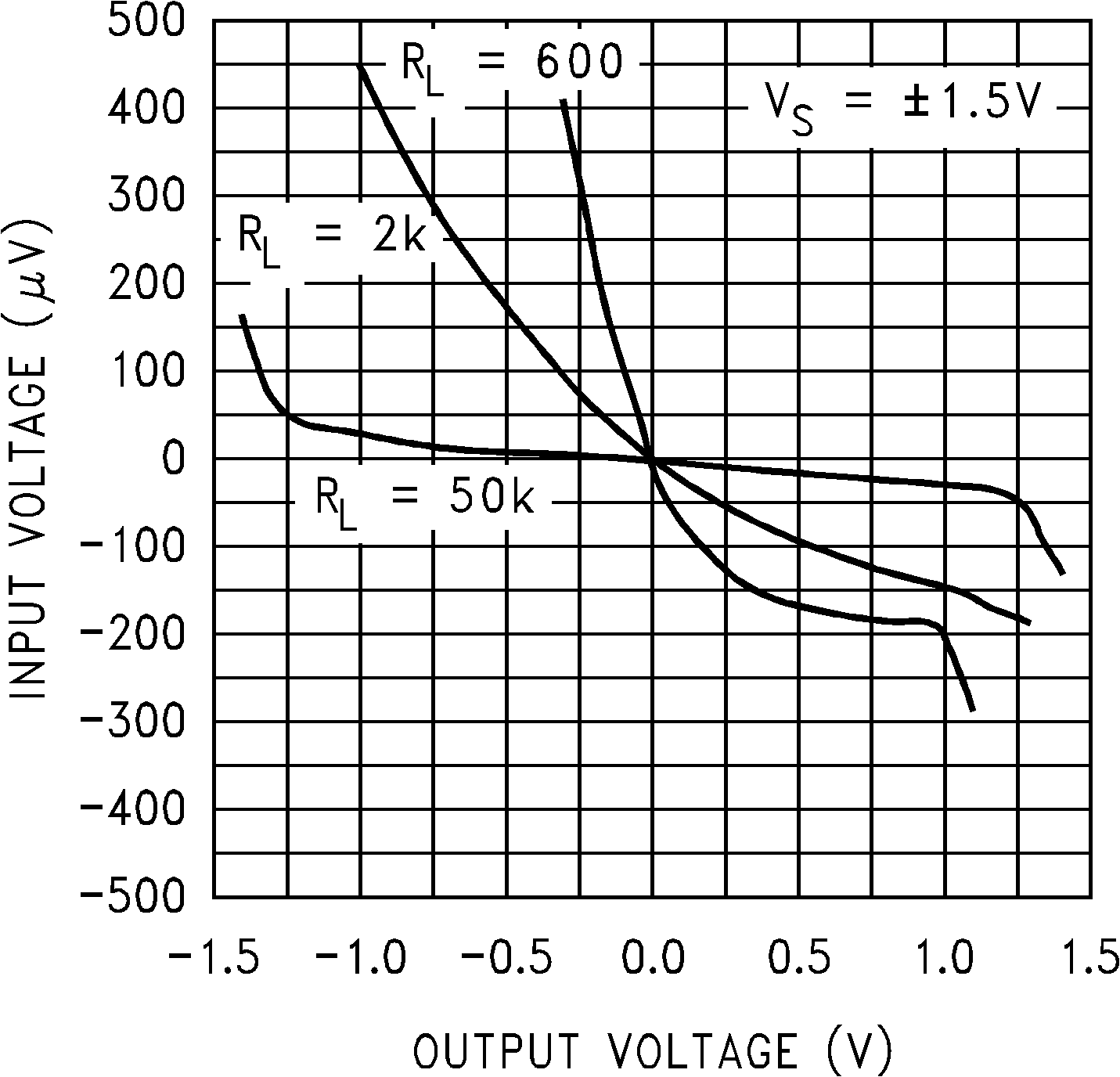 Figure 10. Input Voltage vs Output Voltage
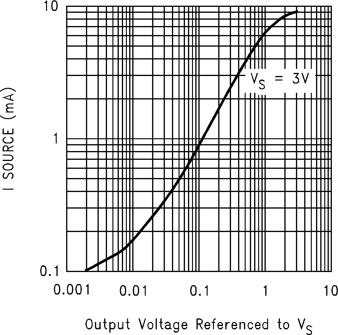 Figure 12. Sourcing Current vs Output Voltage
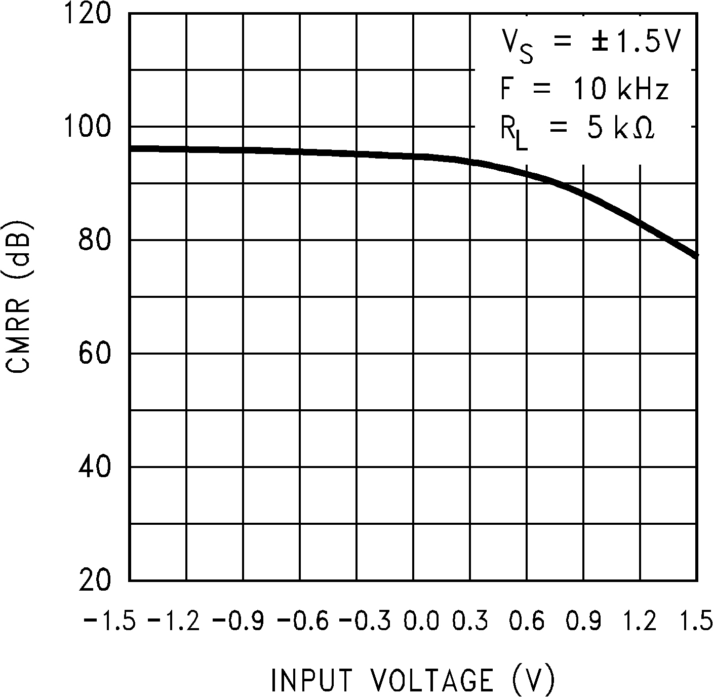
6.12.3 Typical Characteristics: 5 V
V+ = 5 V, V– = 0 V, TA = 25°C, unless otherwise specified.
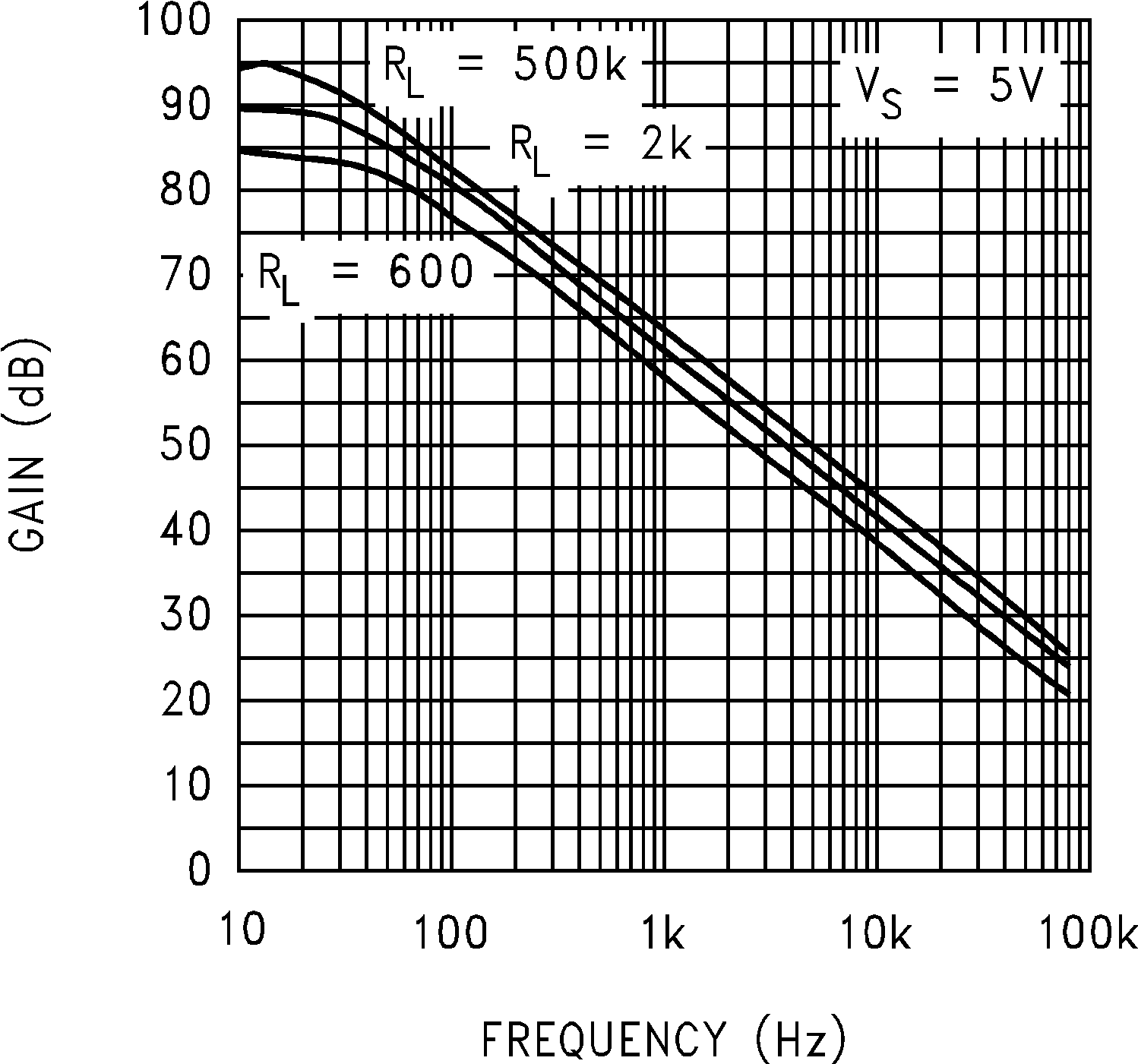 Figure 15. Open Loop Frequency Response
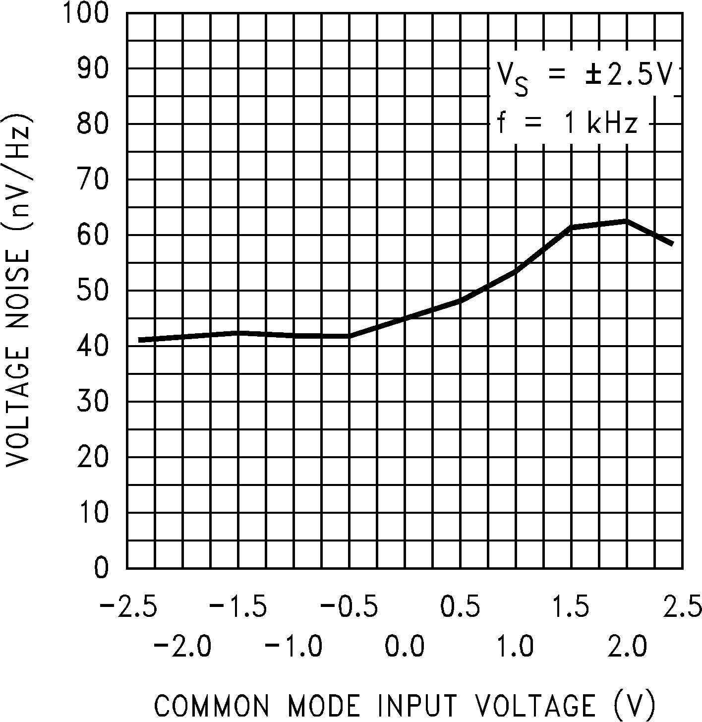 Figure 17. Input Voltage Noise vs Input Voltage
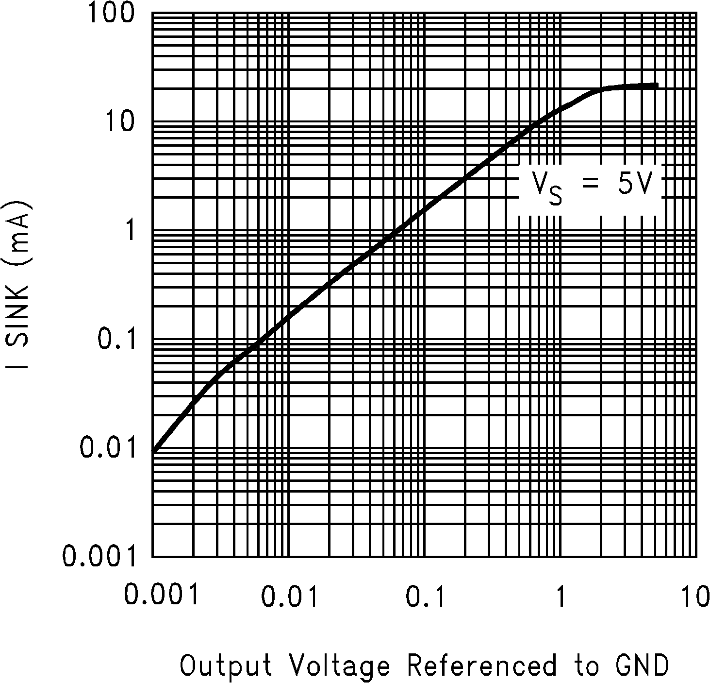 Figure 19. Sinking Current vs Output Voltage
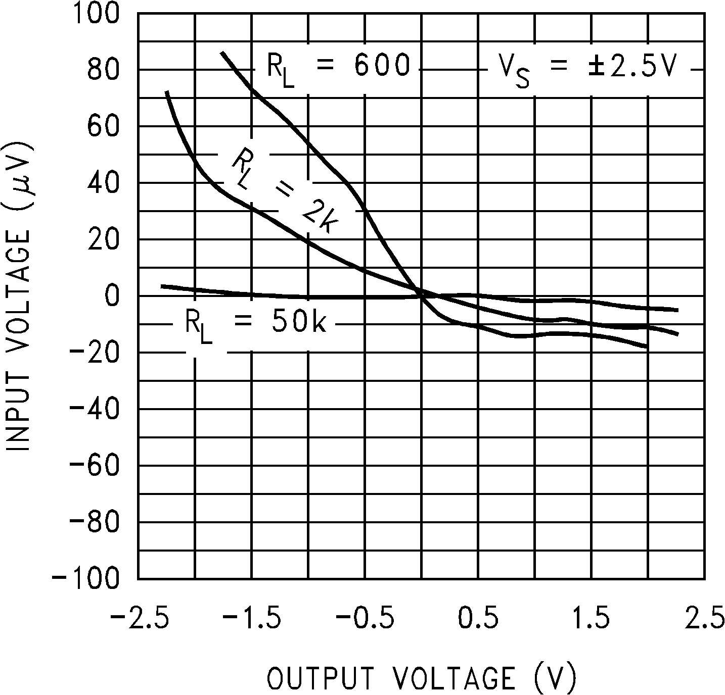 Figure 16. Input Voltage vs Output Voltage
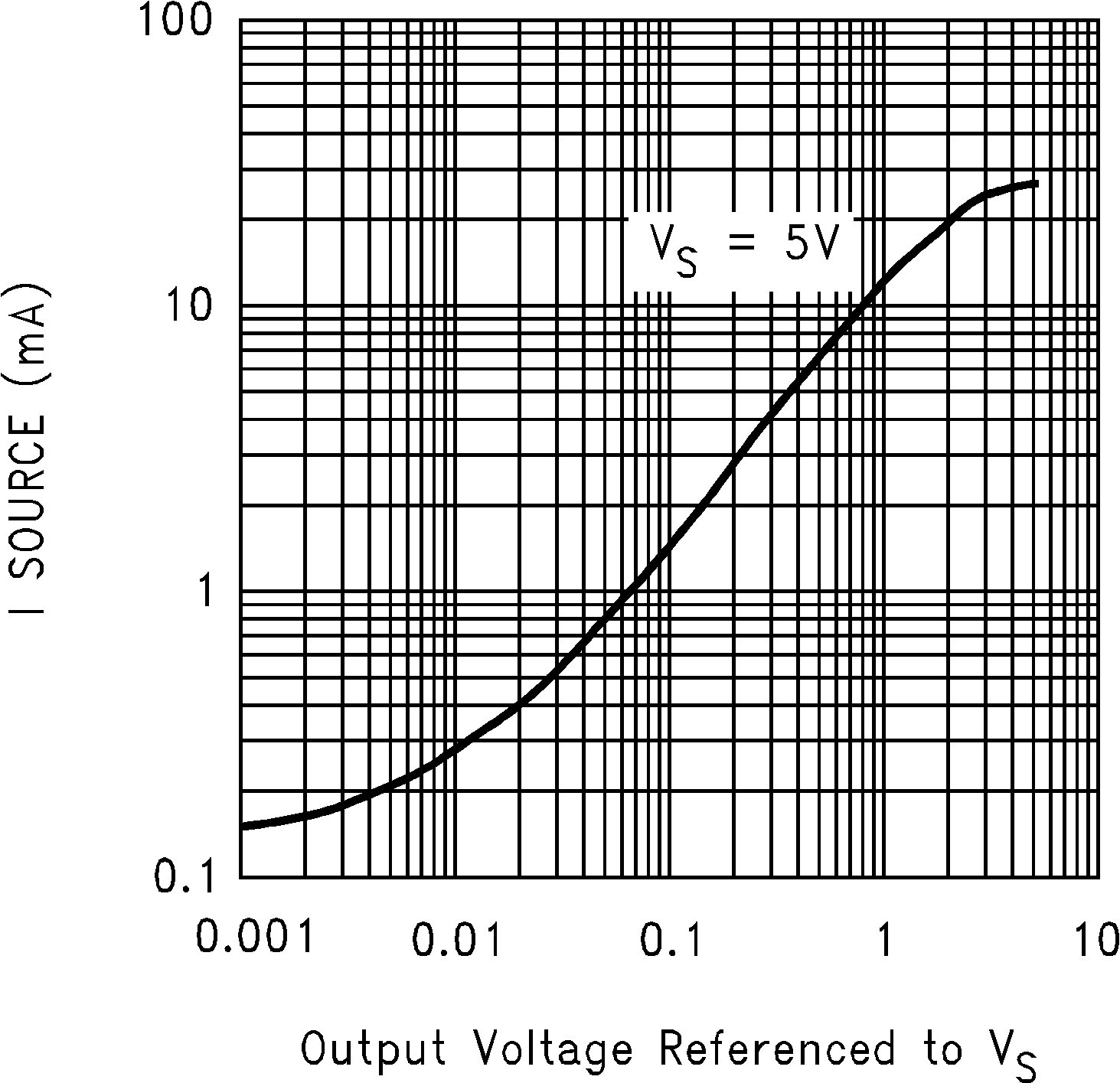
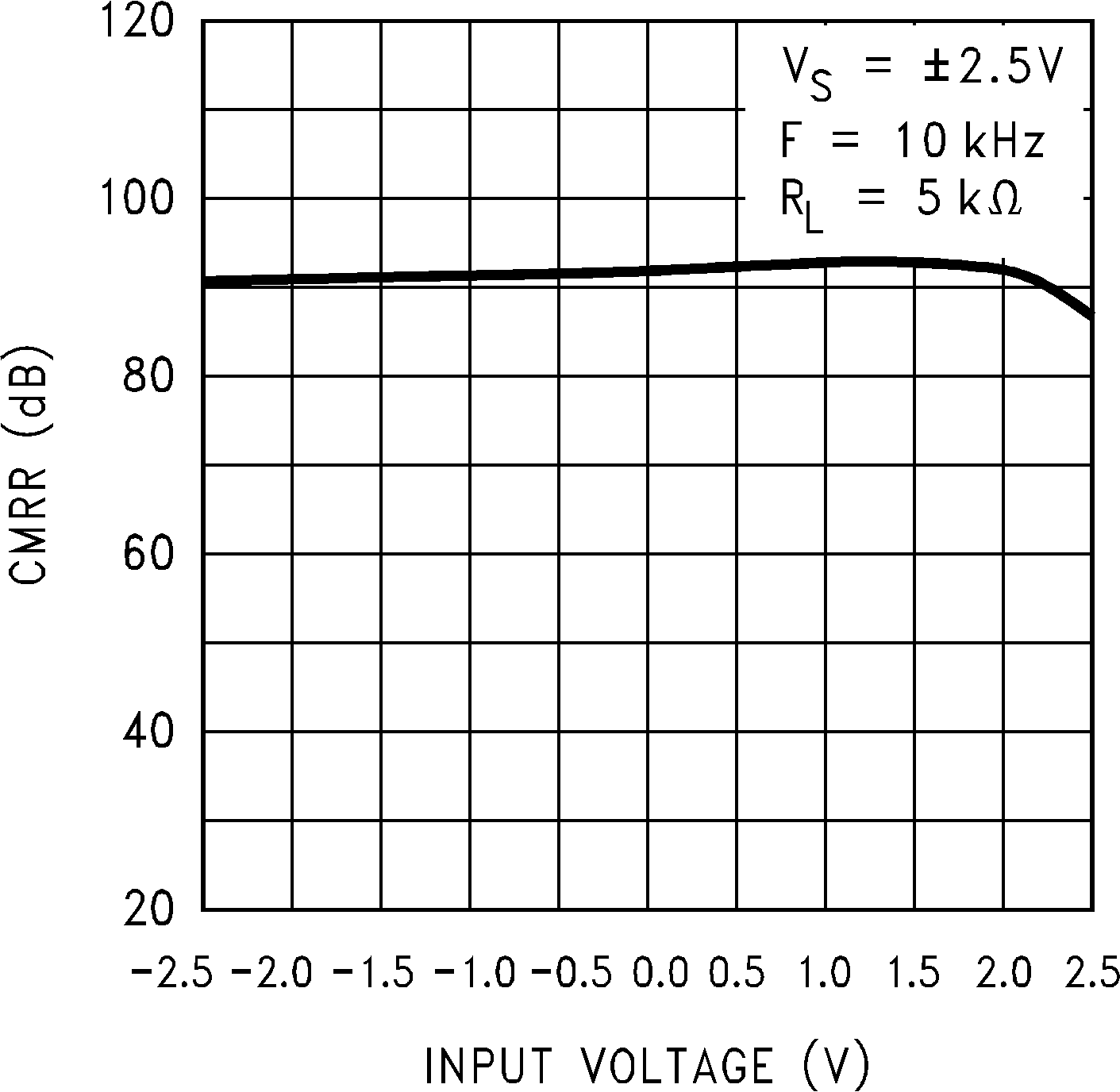 Figure 20. CMRR vs Input Voltage
6.12.4 Typical Characteristics: 15 V
V+ = +15 V, V– = 0 V, TA = 25°C, unless otherwise specified.
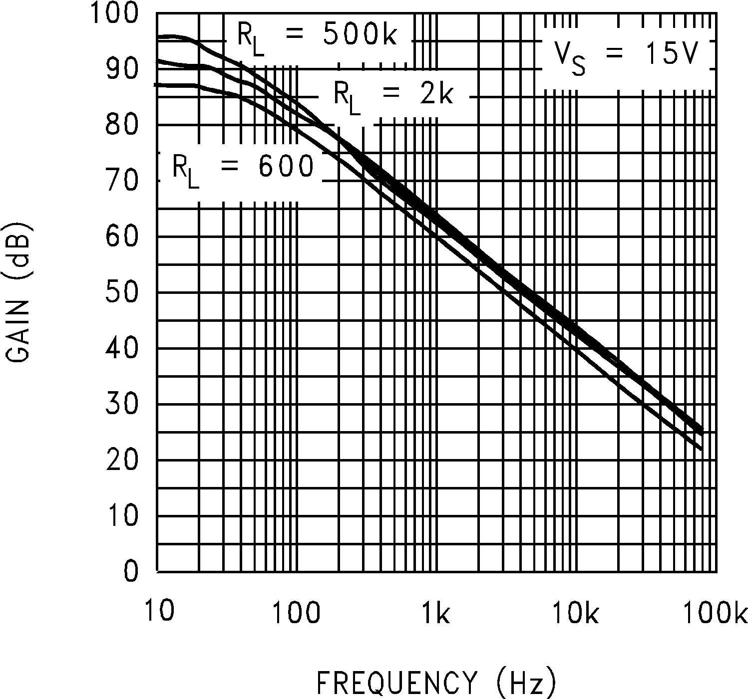 Figure 21. Open Loop Frequency Response
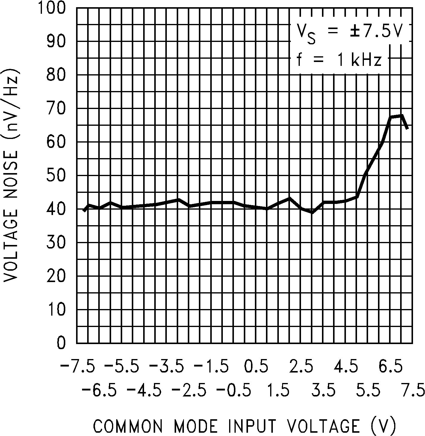 Figure 23. Input Voltage Noise vs Input Voltage
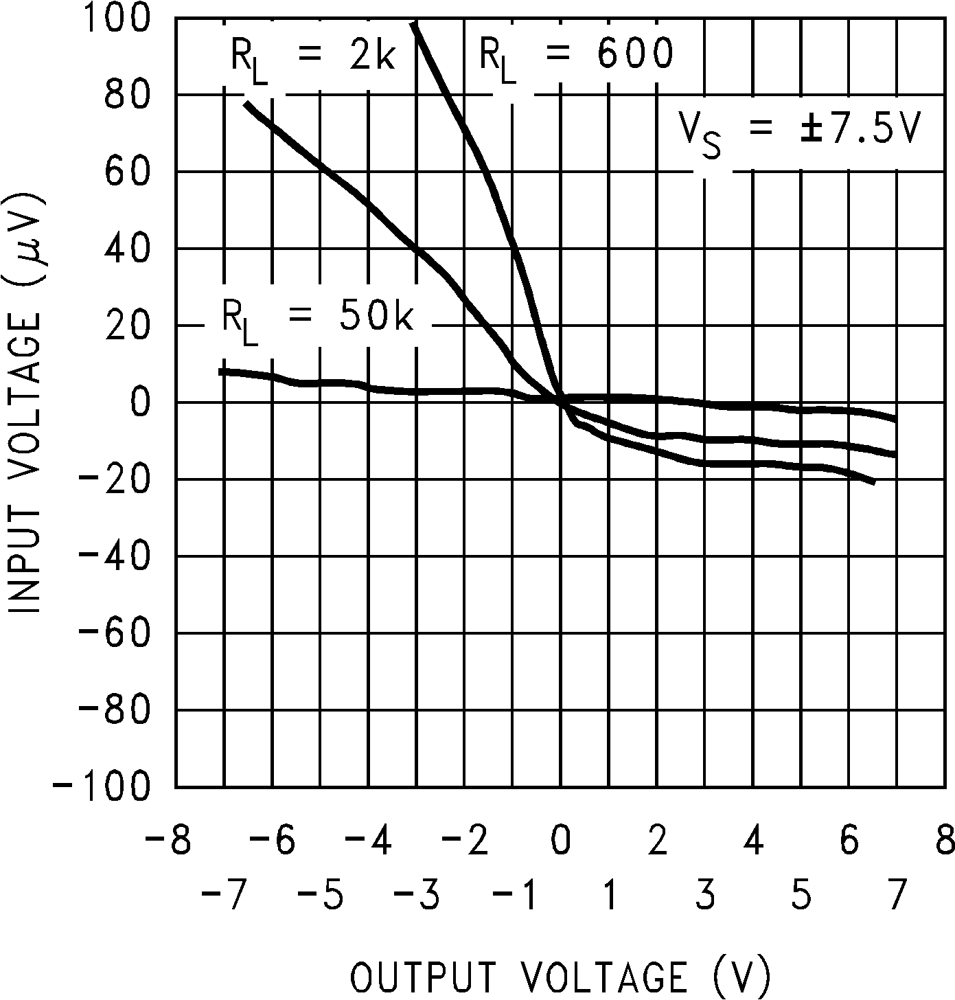 Figure 22. Input Voltage vs Output Voltage
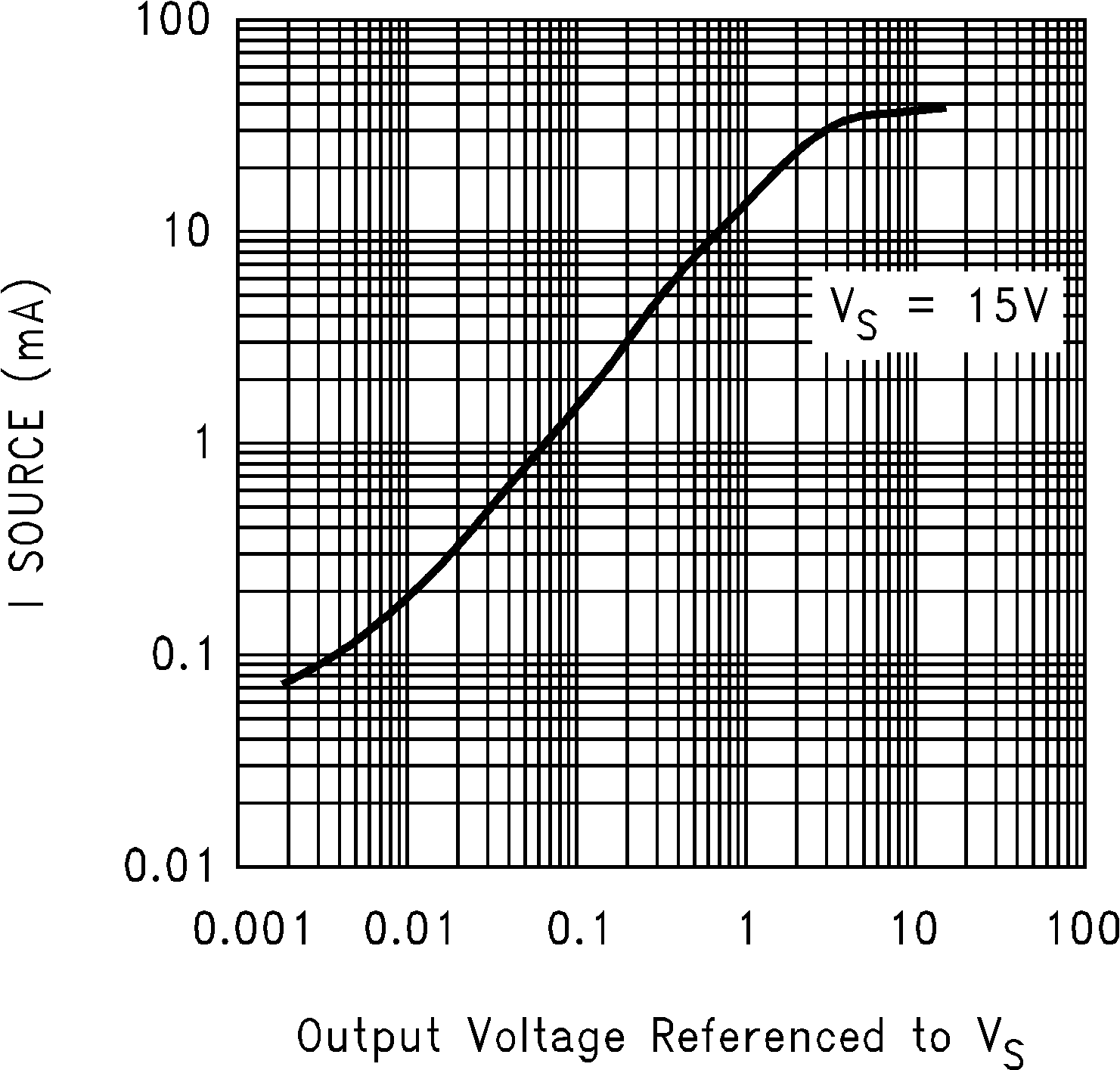 Figure 24. Sourcing Current vs Output Voltage
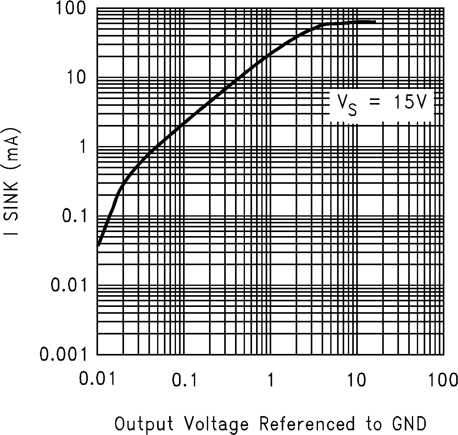 Figure 25. Sinking Current vs Output Voltage
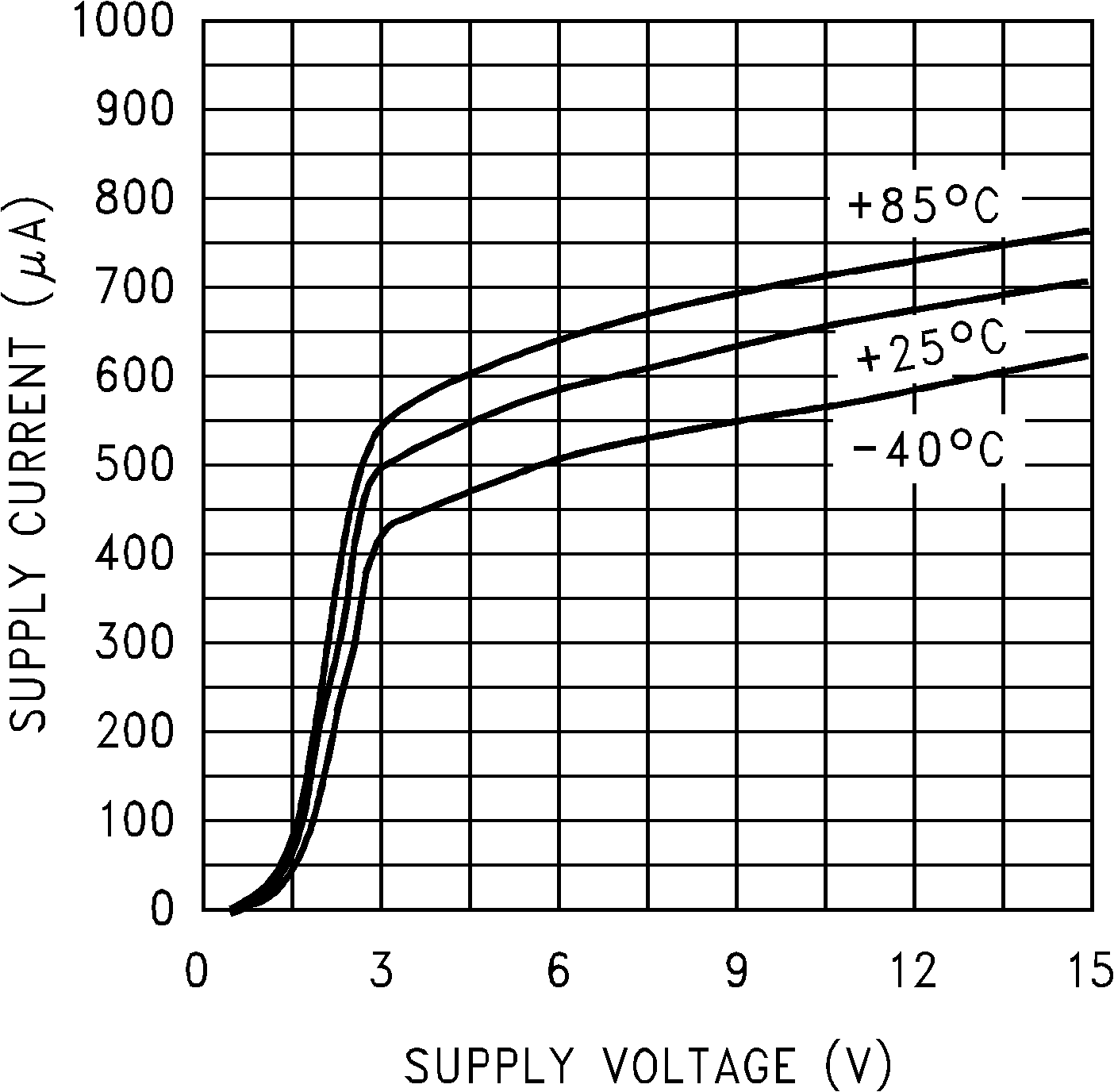 Figure 27. Supply Current vs Supply Voltage
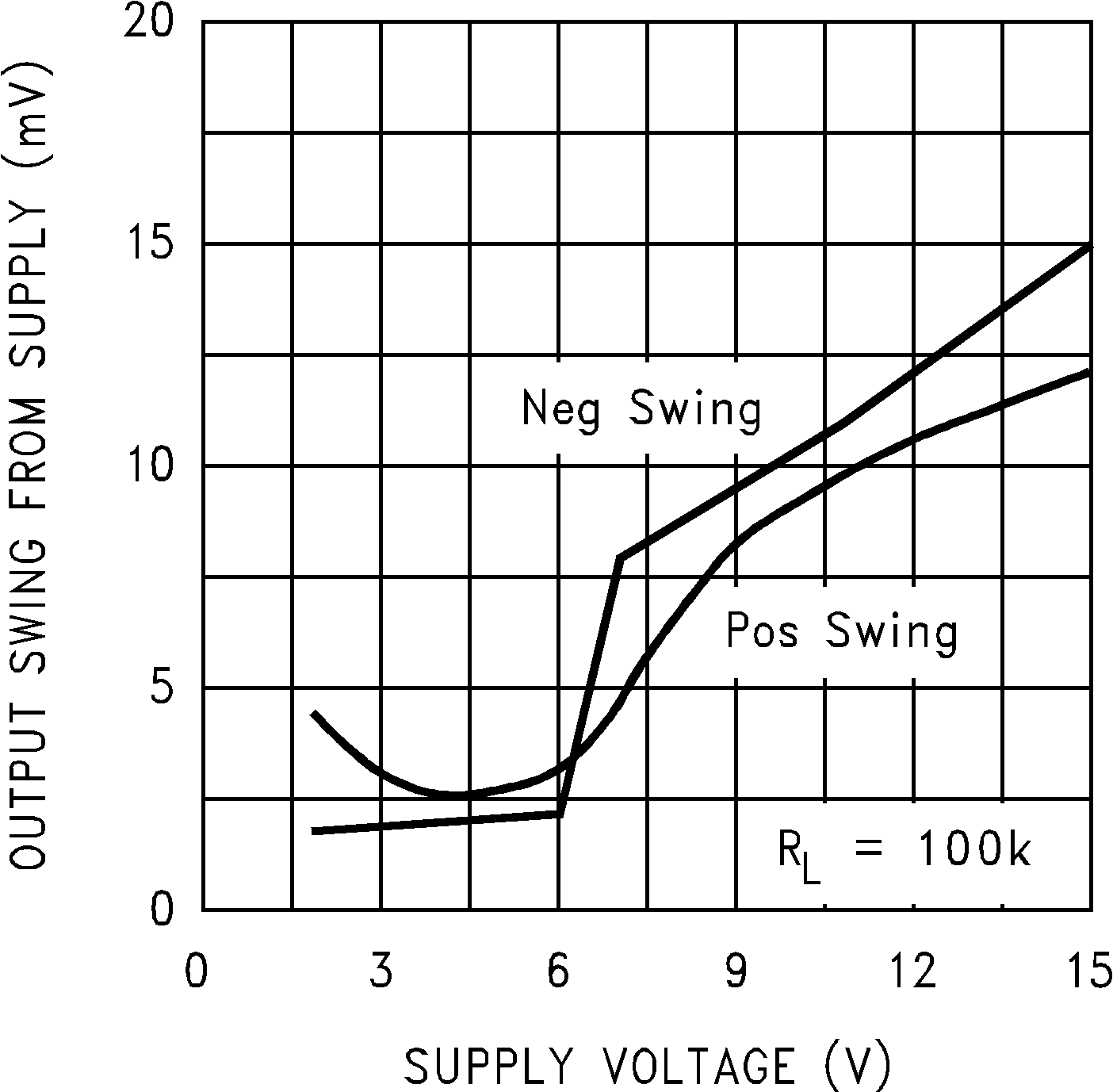 Figure 29. Output Voltage Swing vs Supply Voltage
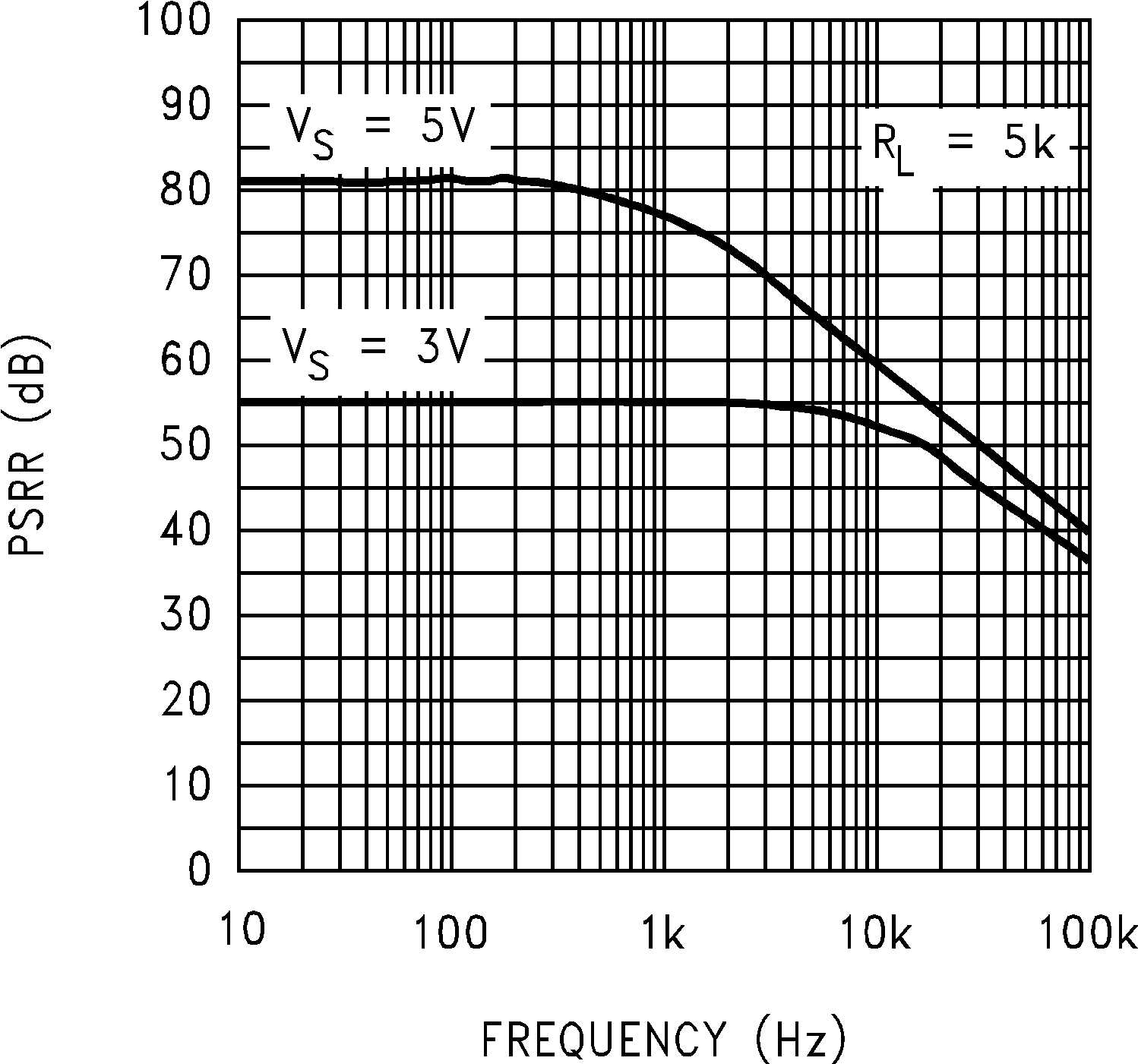 Figure 31. Positive PSRR vs Frequency
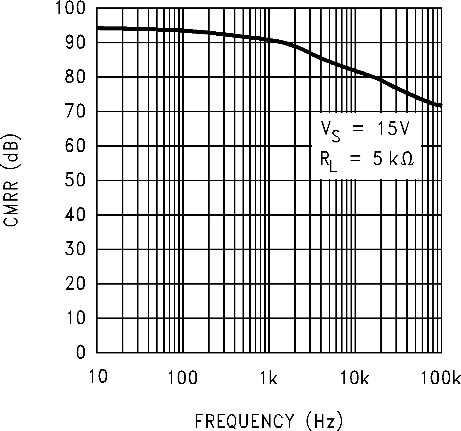 Figure 33. CMRR vs Frequency
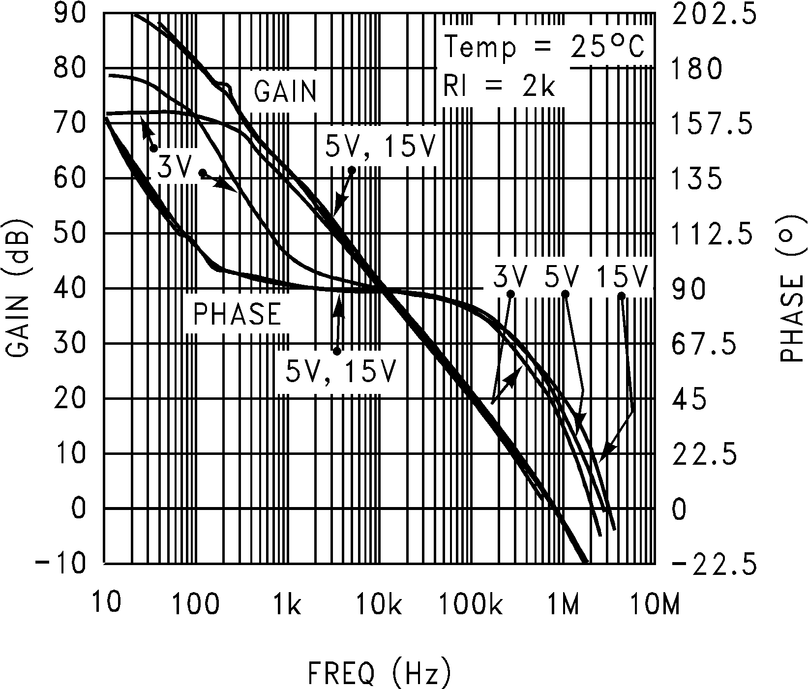 Figure 35. Open Loop Frequency Response at 25°C
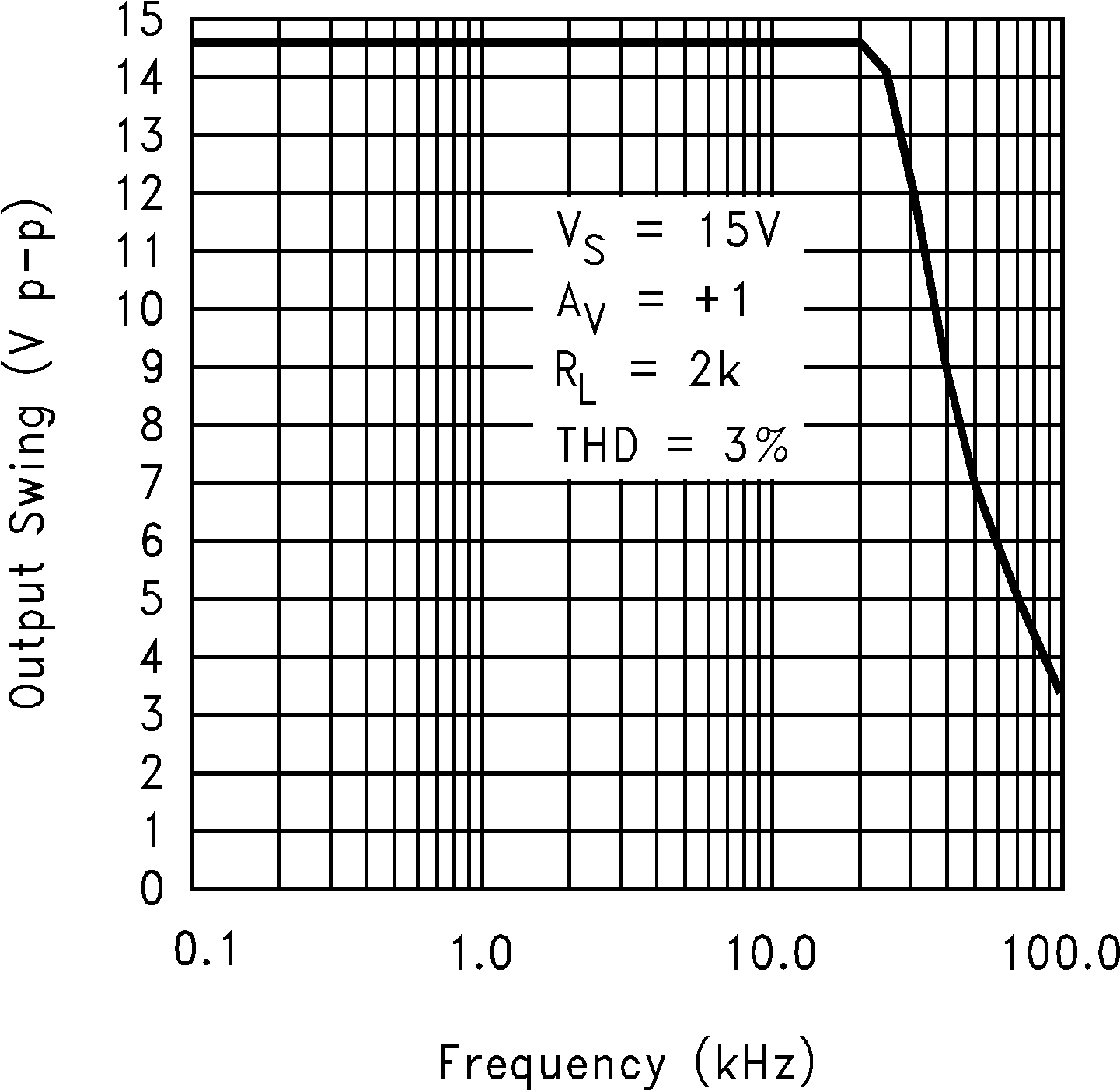 Figure 37. Maximum Output Swing vs Frequency
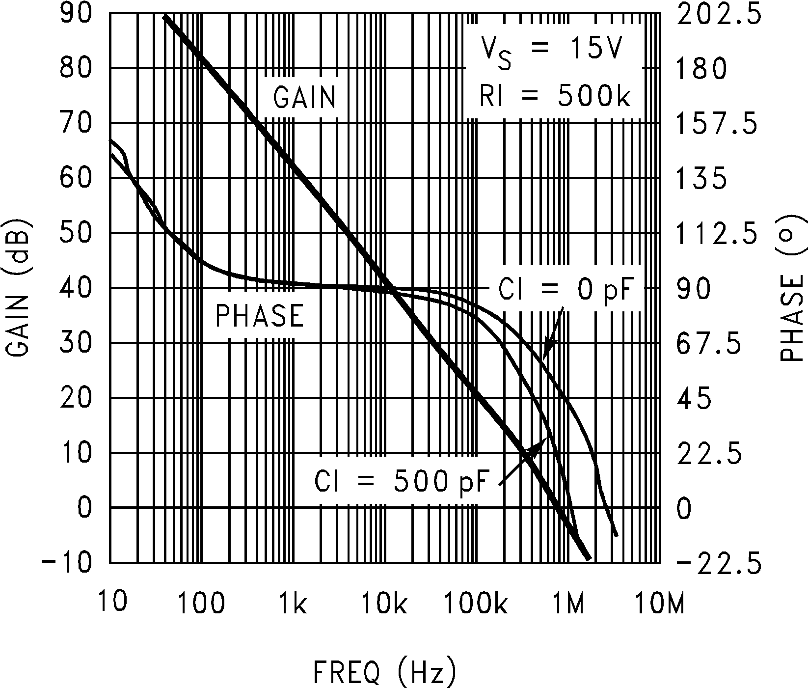 Figure 39. Gain and Phase vs Capacitive Load
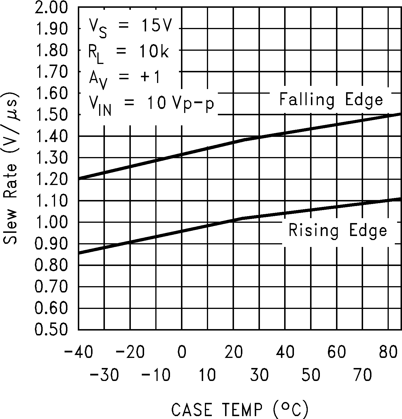 Figure 41. Slew Rate vs Temperature
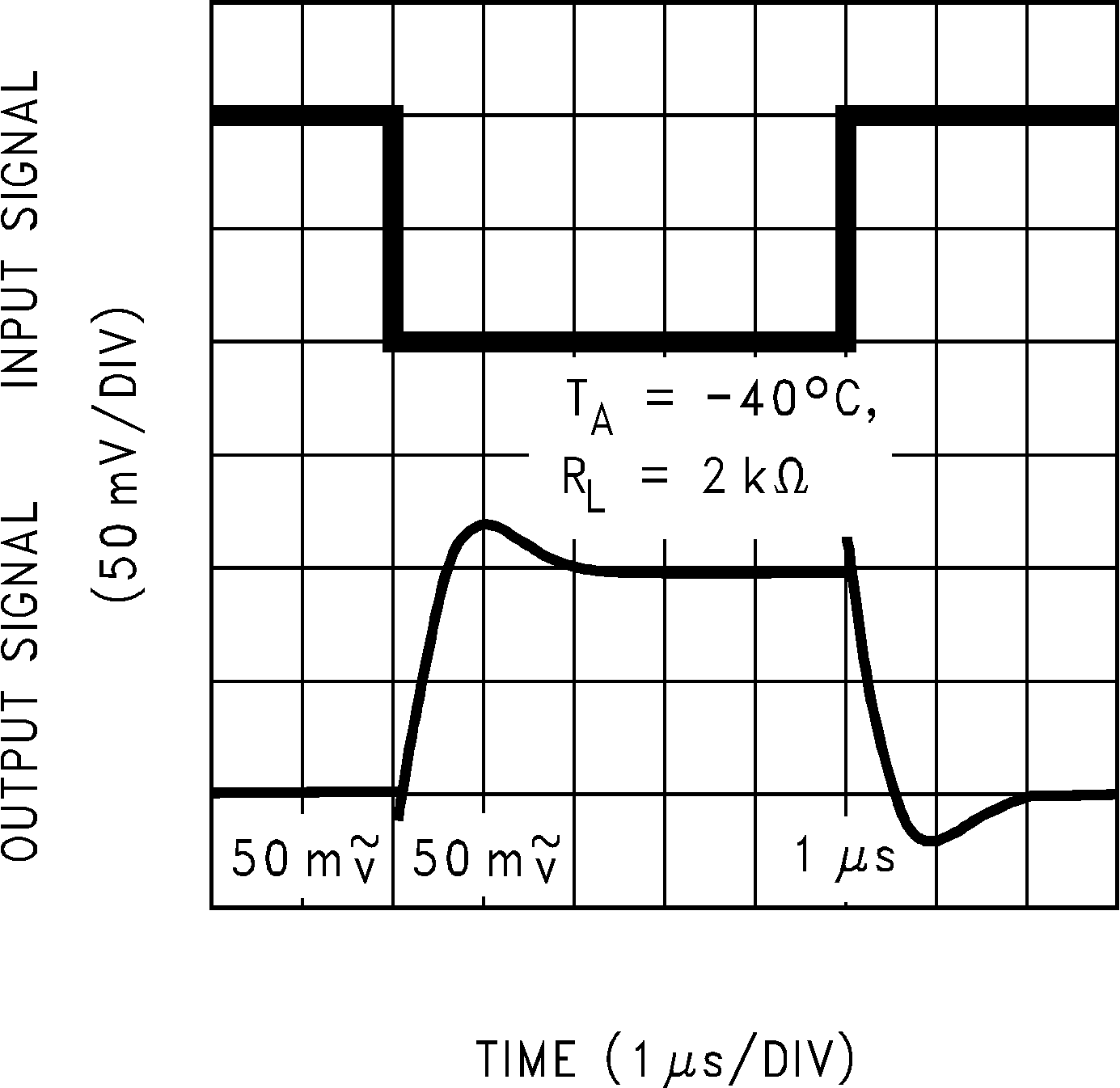 Figure 43. Inverting Small Signal Pulse Response
 Figure 45. Inverting Small Signal Pulse Response
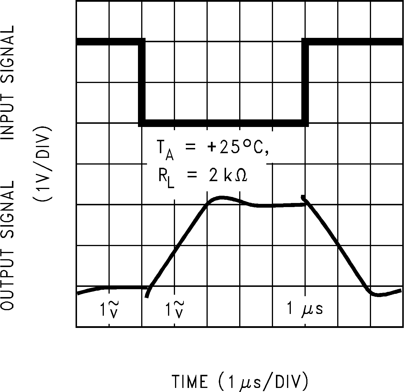 Figure 47. Inverting Large Signal Pulse Response
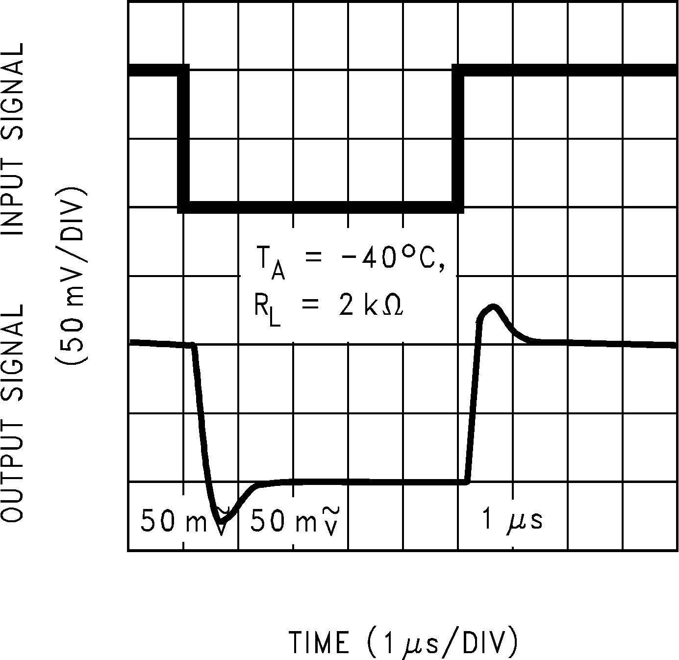 Figure 49. Noninverting Small Signal Pulse Response
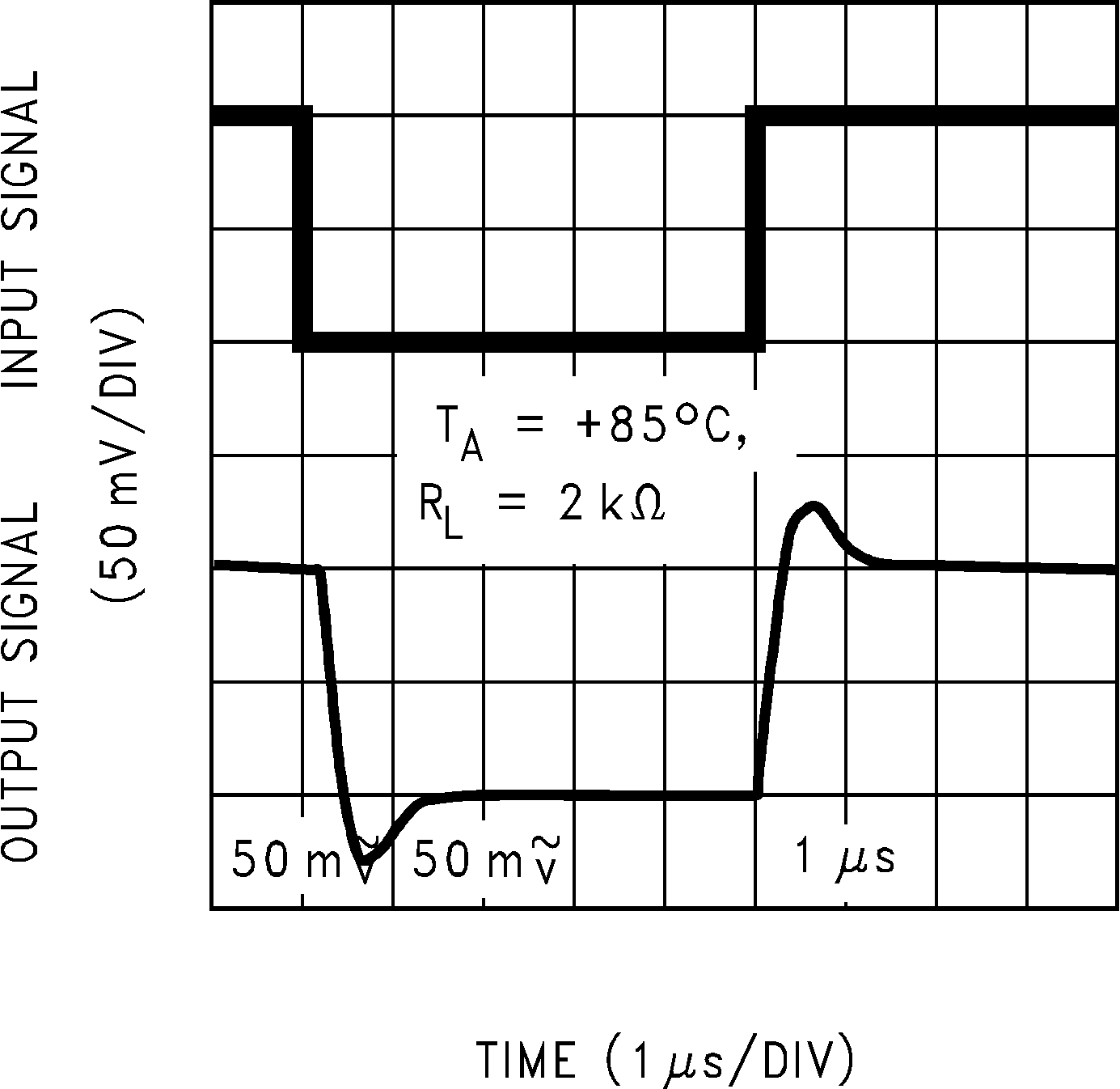 Figure 51. Noninverting Small Signal Pulse Response
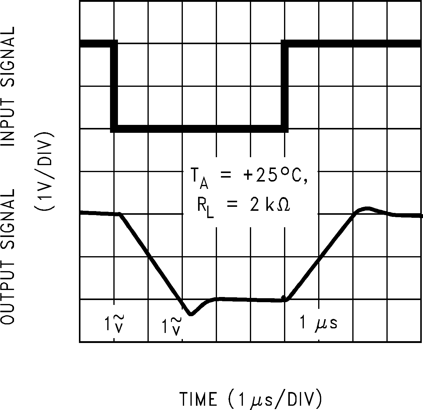 Figure 53. Noninverting Large Signal Pulse Response
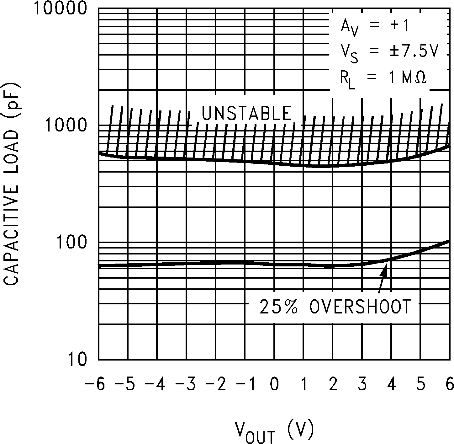 Figure 55. Stability vs Capacitive Load
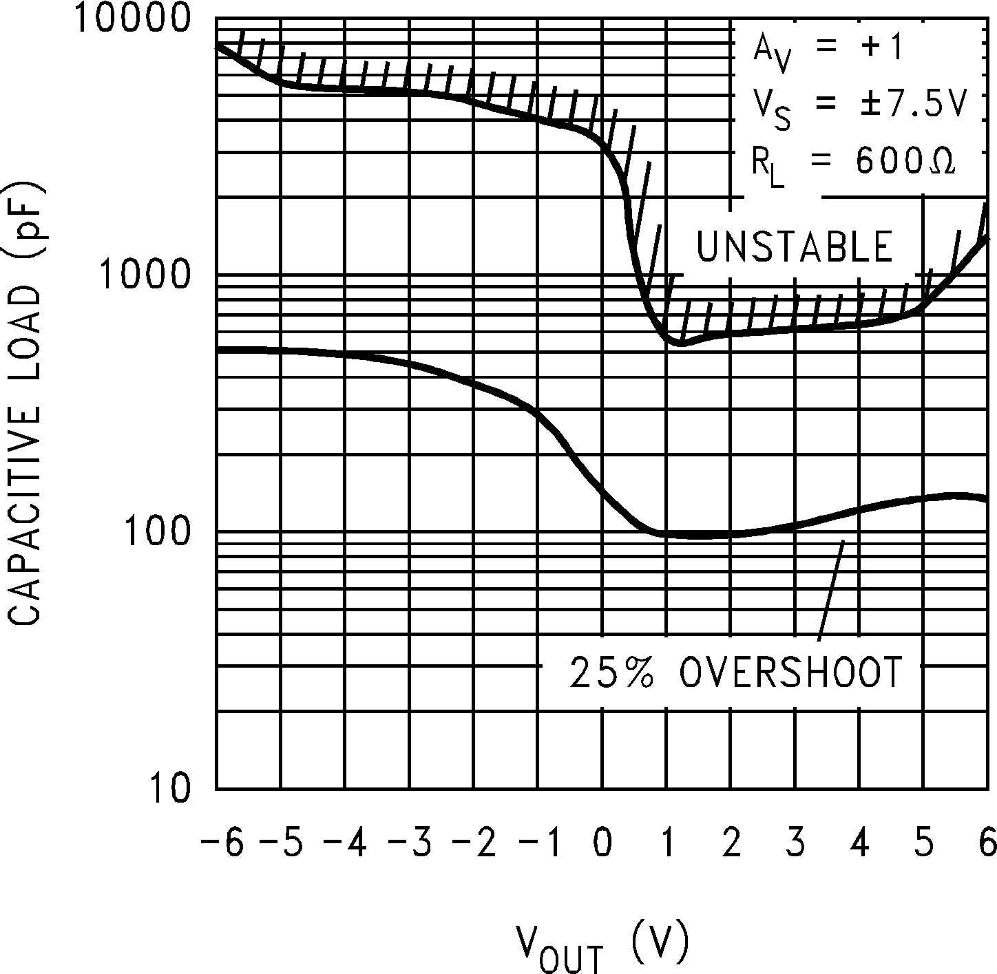 Figure 57. Stability vs Capacitive Load
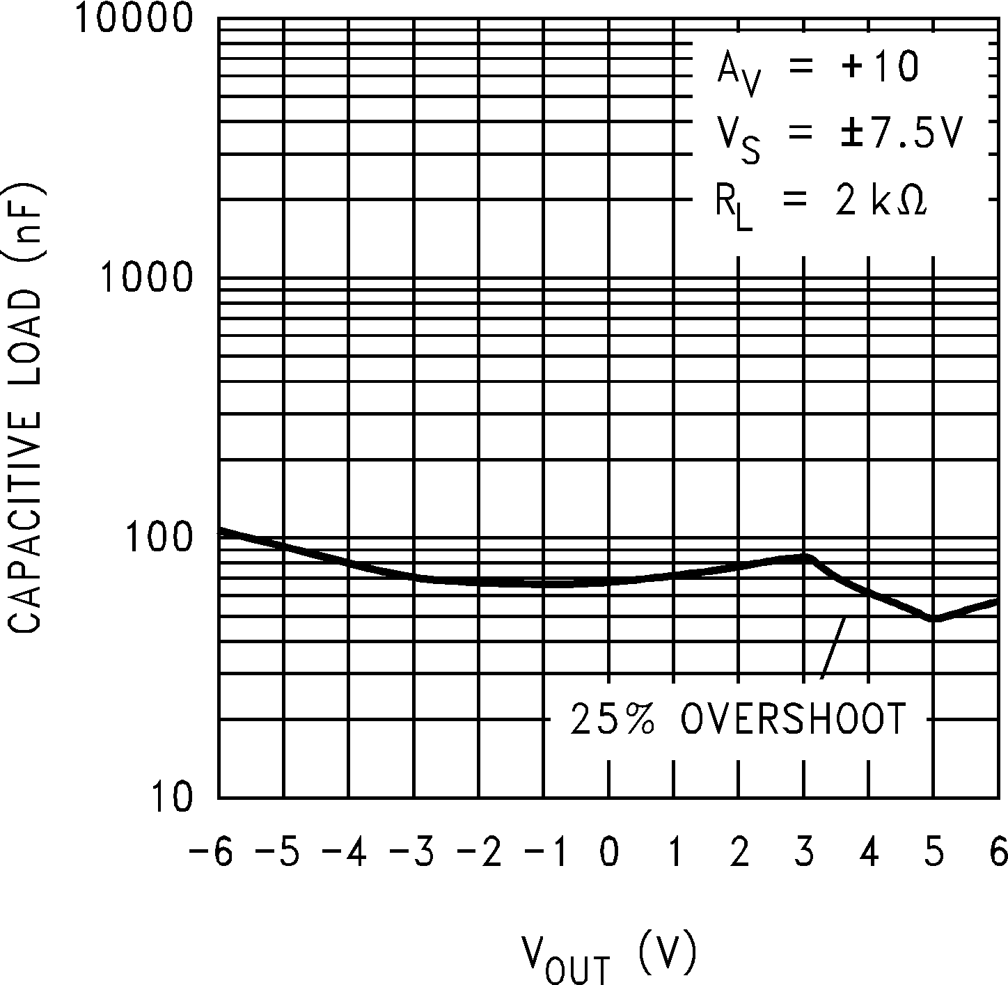 Figure 59. Stability vs Capacitive Load
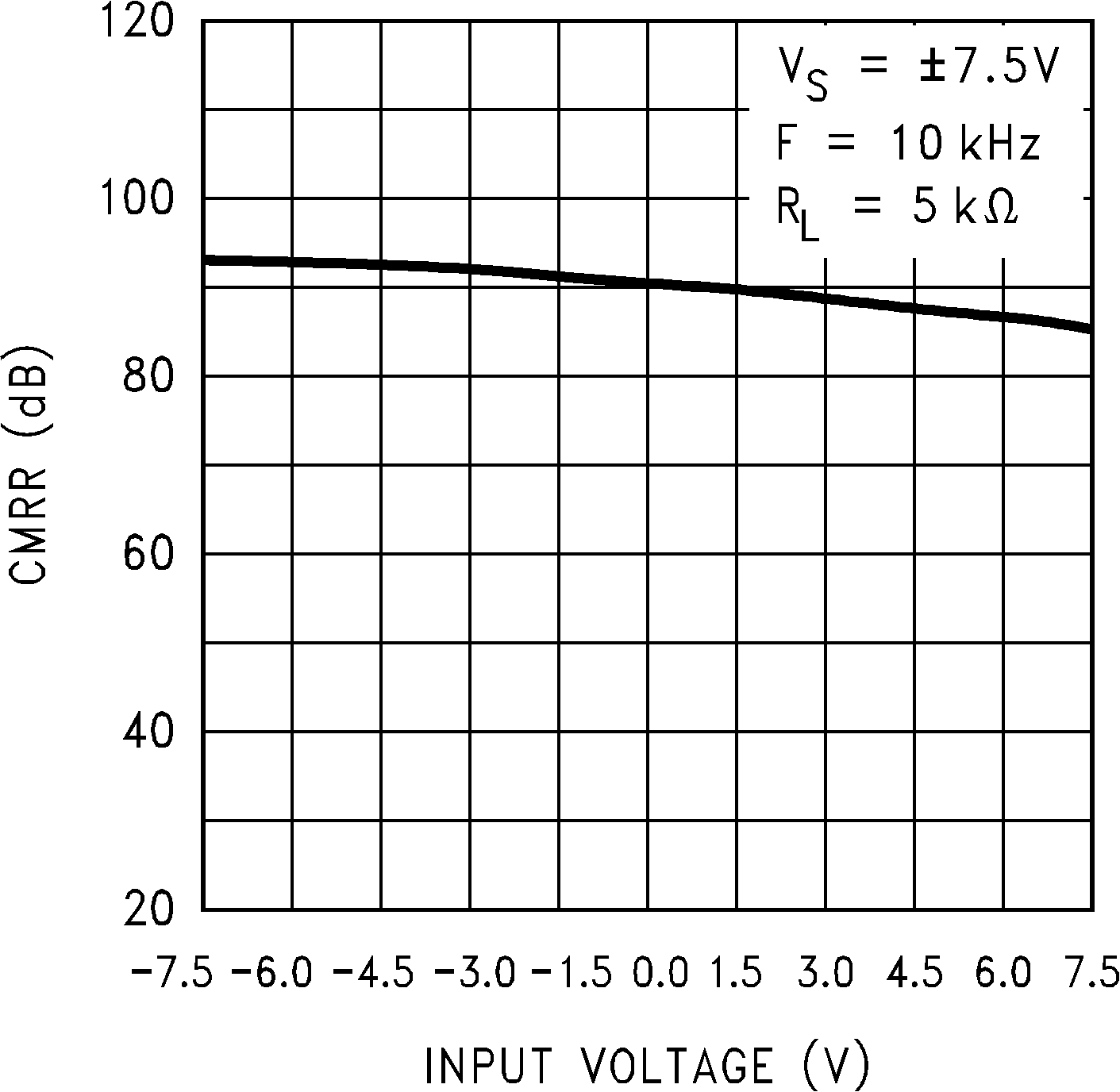
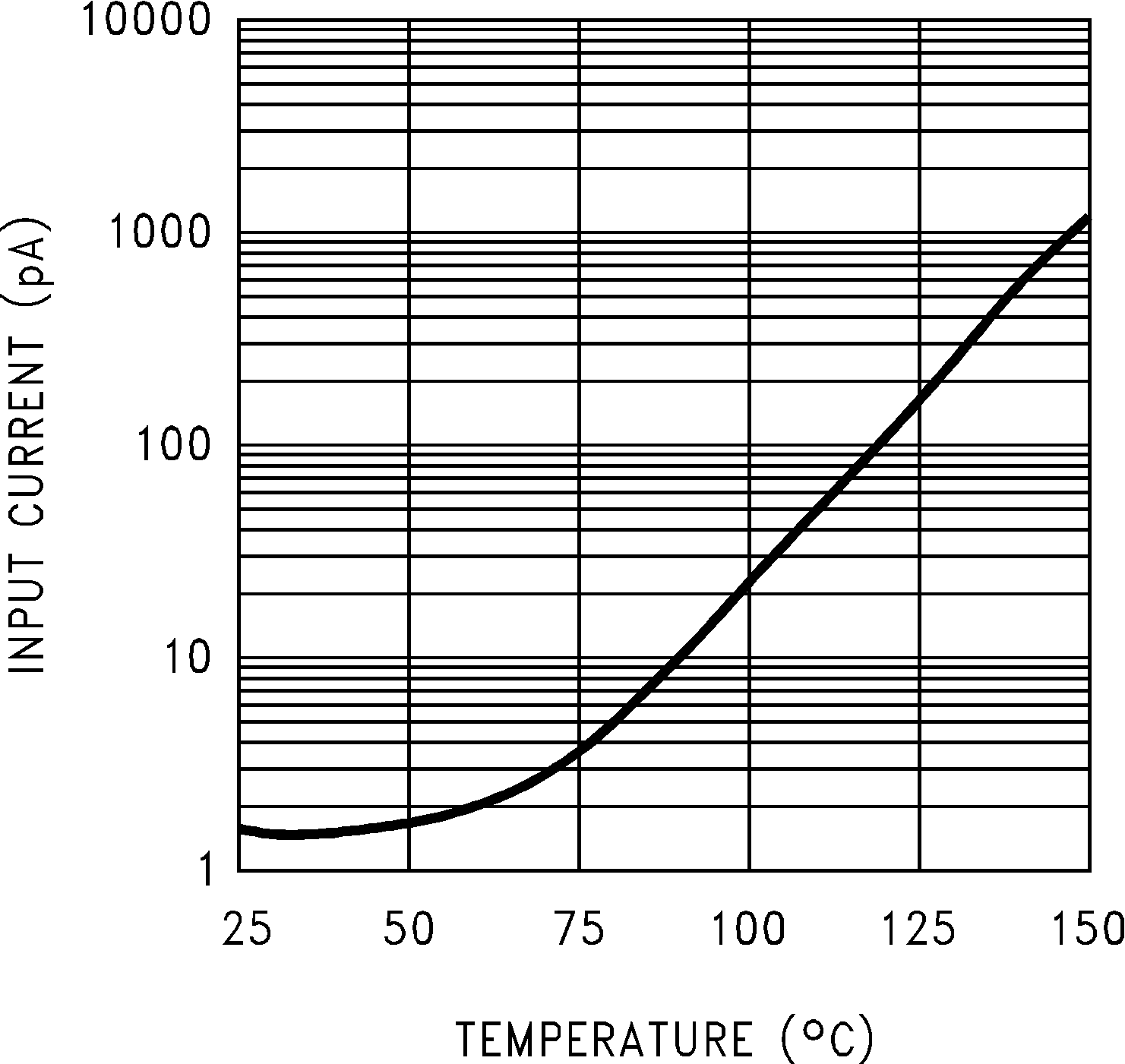 Figure 28. Input Current vs Temperature
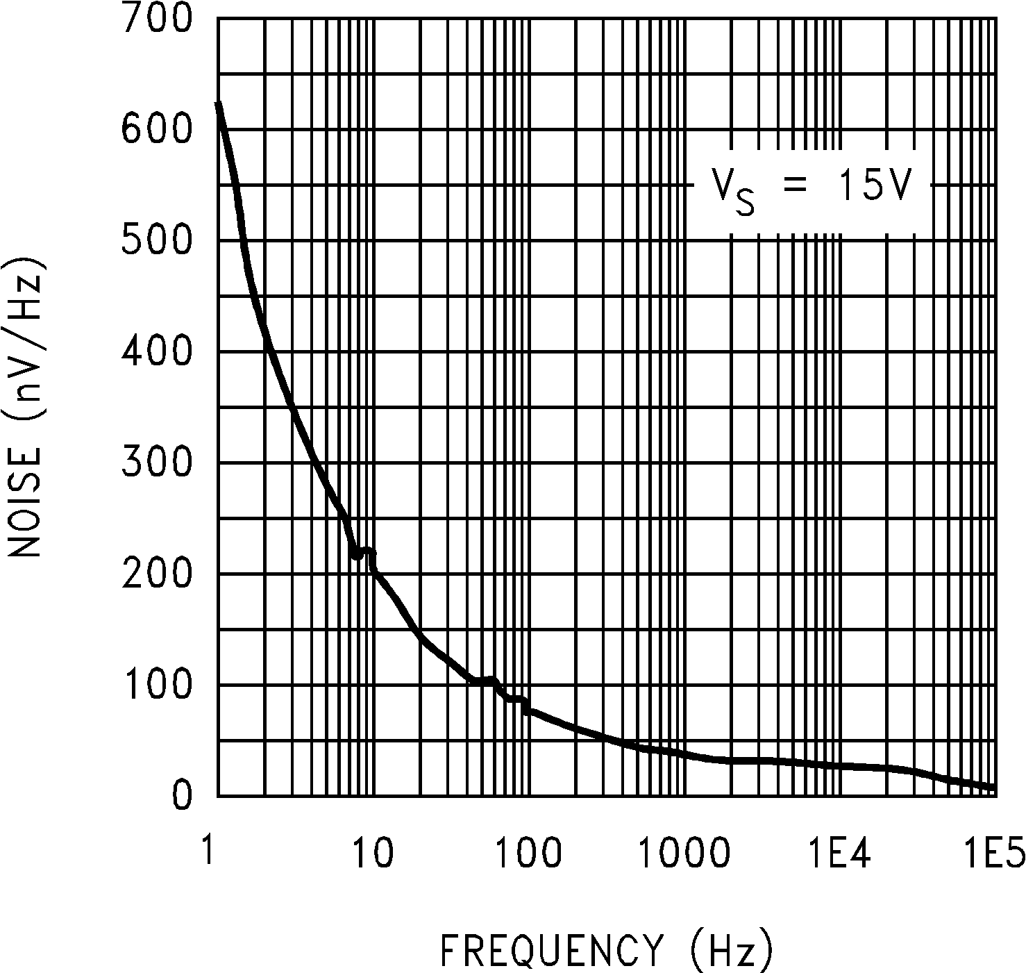 Figure 30. Input Voltage Noise vs Frequency
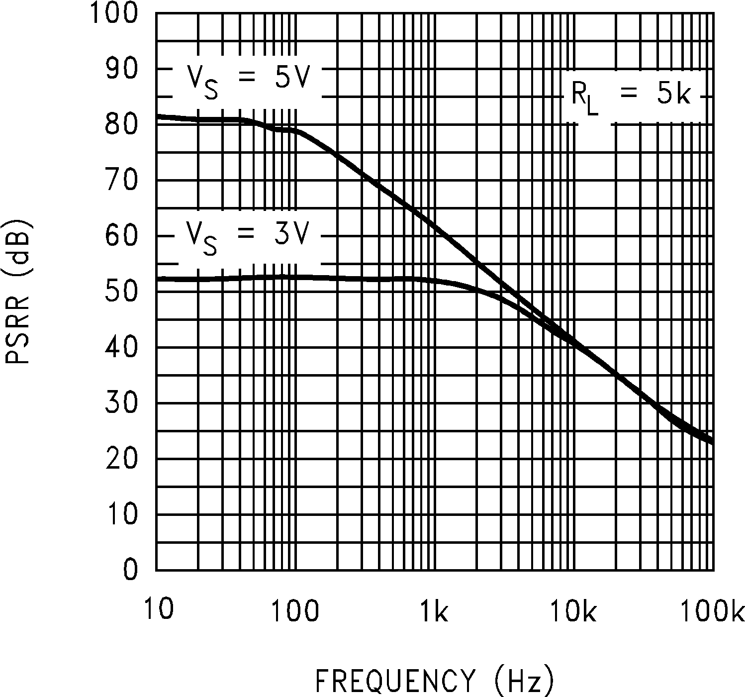 Figure 32. Negative PSRR vs Frequency
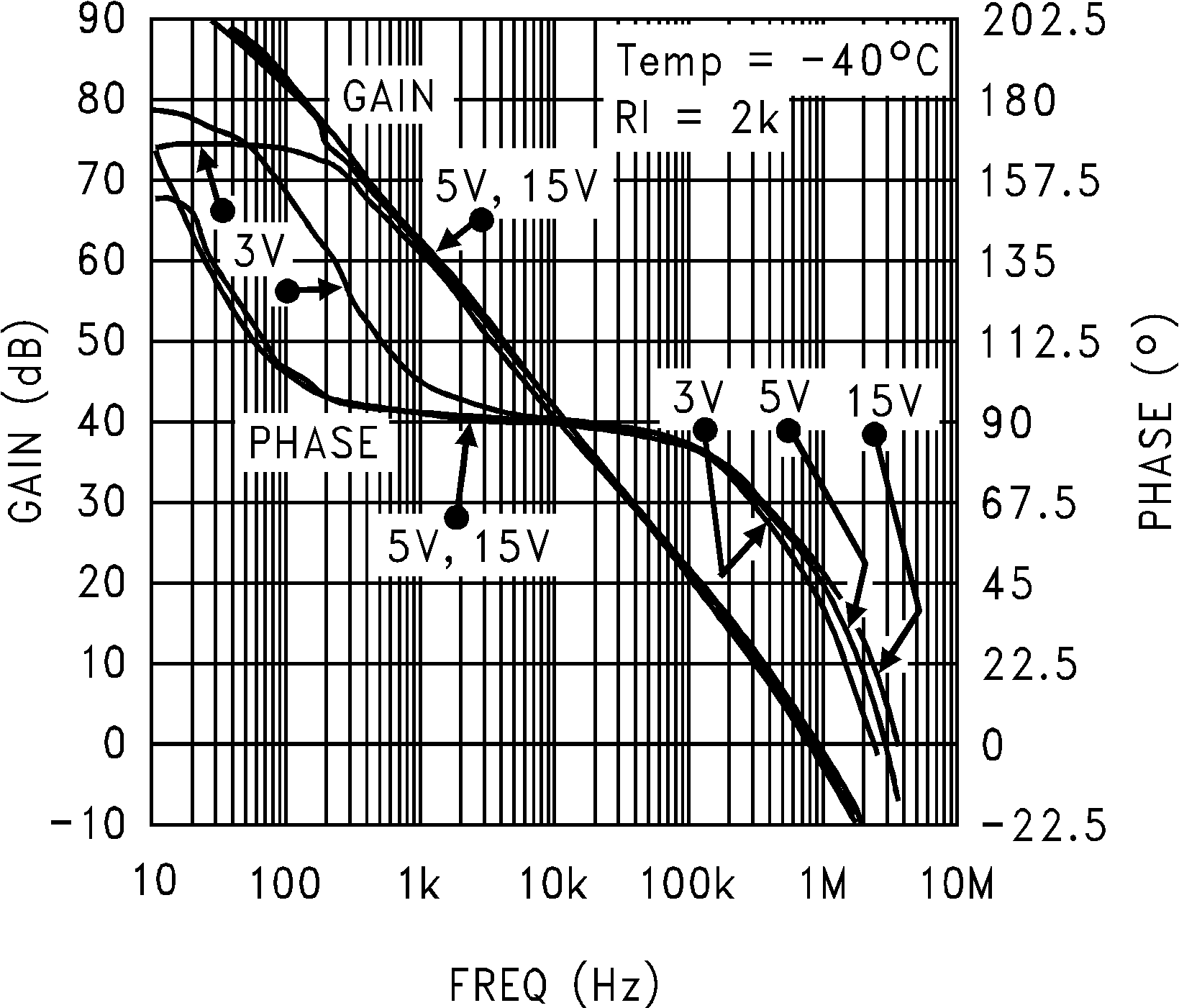 Figure 34. Open Loop Frequency Response at –40°C
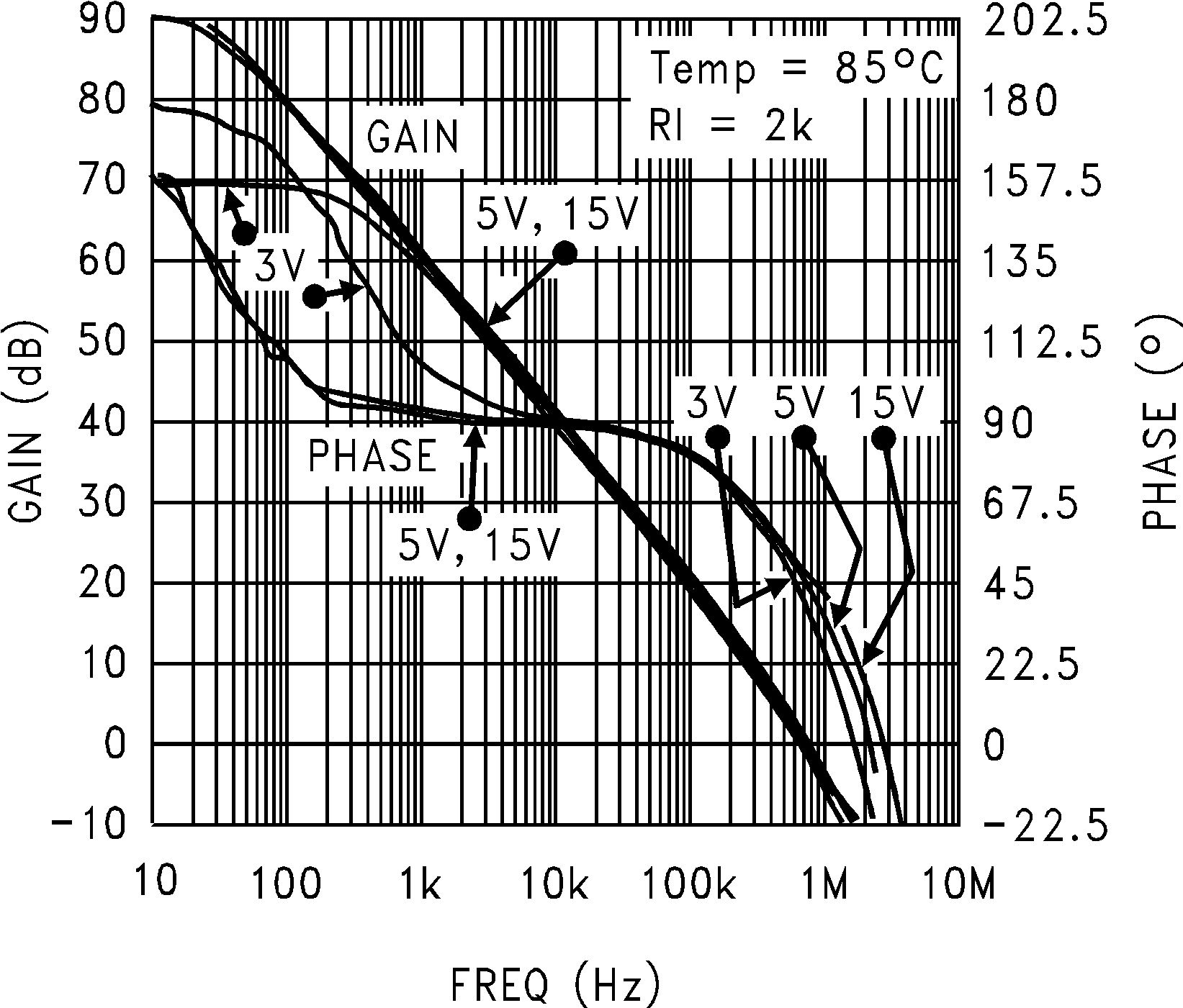 Figure 36. Open Loop Frequency Response at 85°C
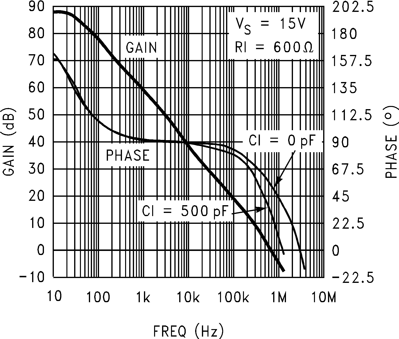 Figure 38. Gain and Phase vs Capacitive Load
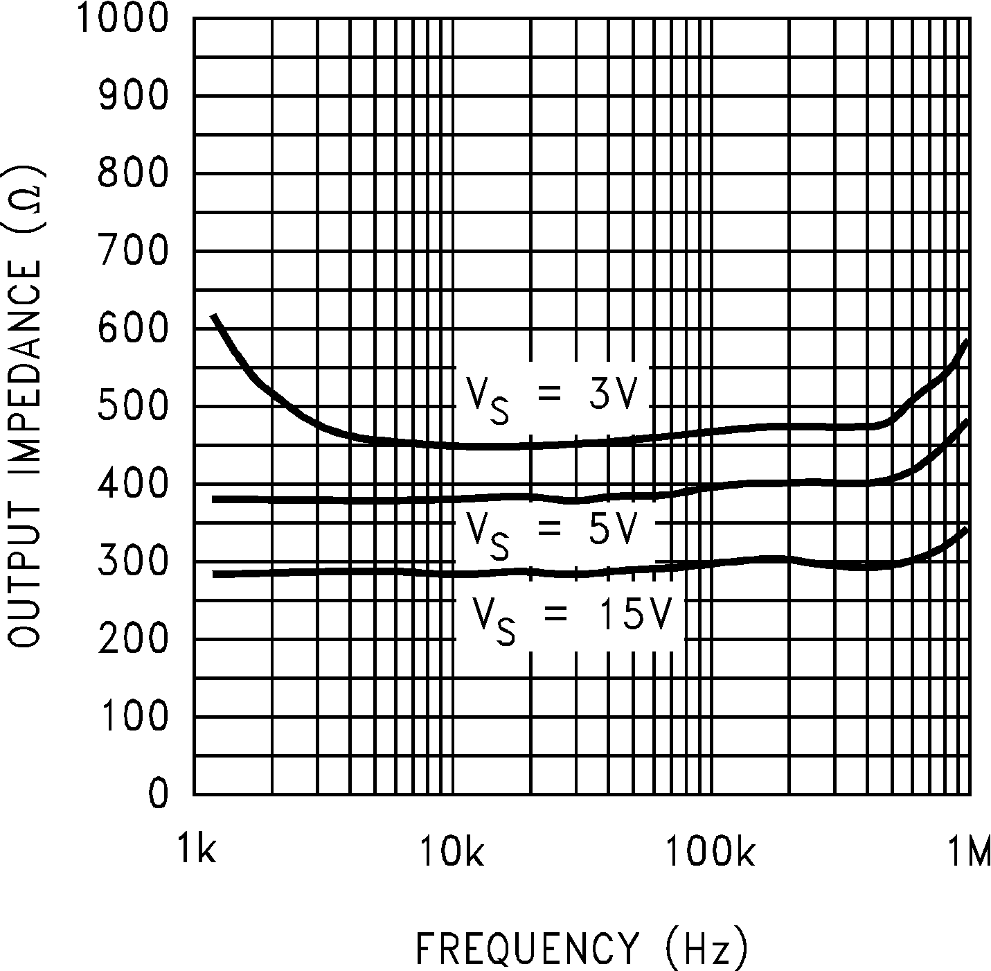 Figure 40. Output Impedance vs Frequency
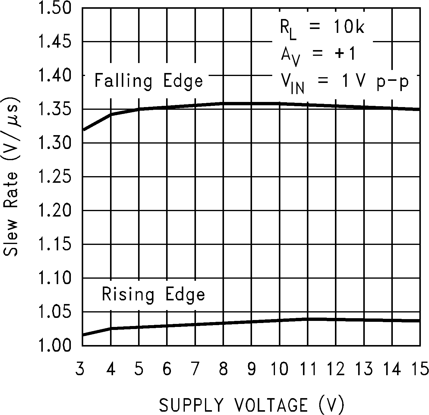 Figure 42. Slew Rate vs Supply Voltage
 Figure 44. Inverting Small Signal Pulse Response
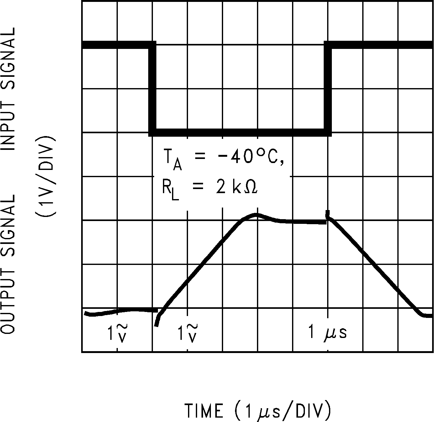 Figure 46. Inverting Large Signal Pulse Response
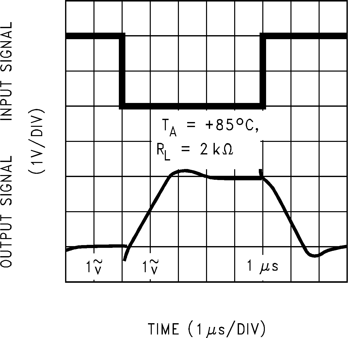 Figure 48. Inverting Large Signal Pulse Response
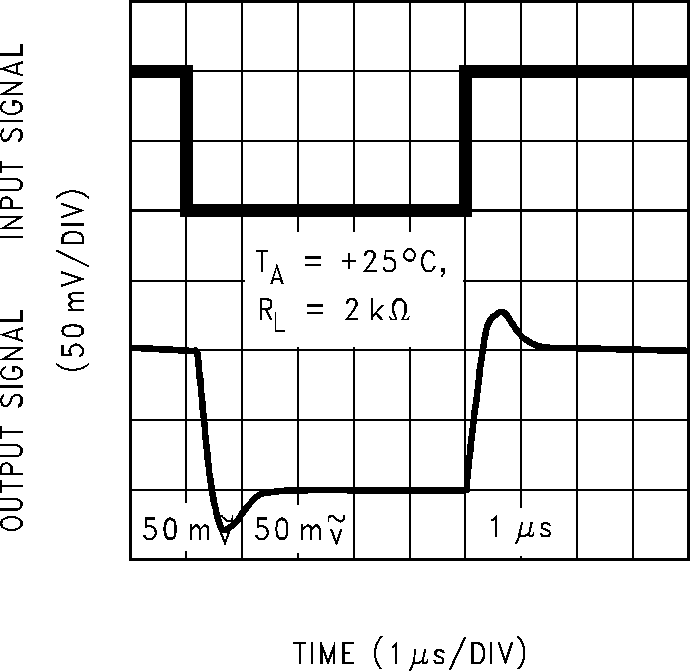 Figure 50. Noninverting Small Signal Pulse Response
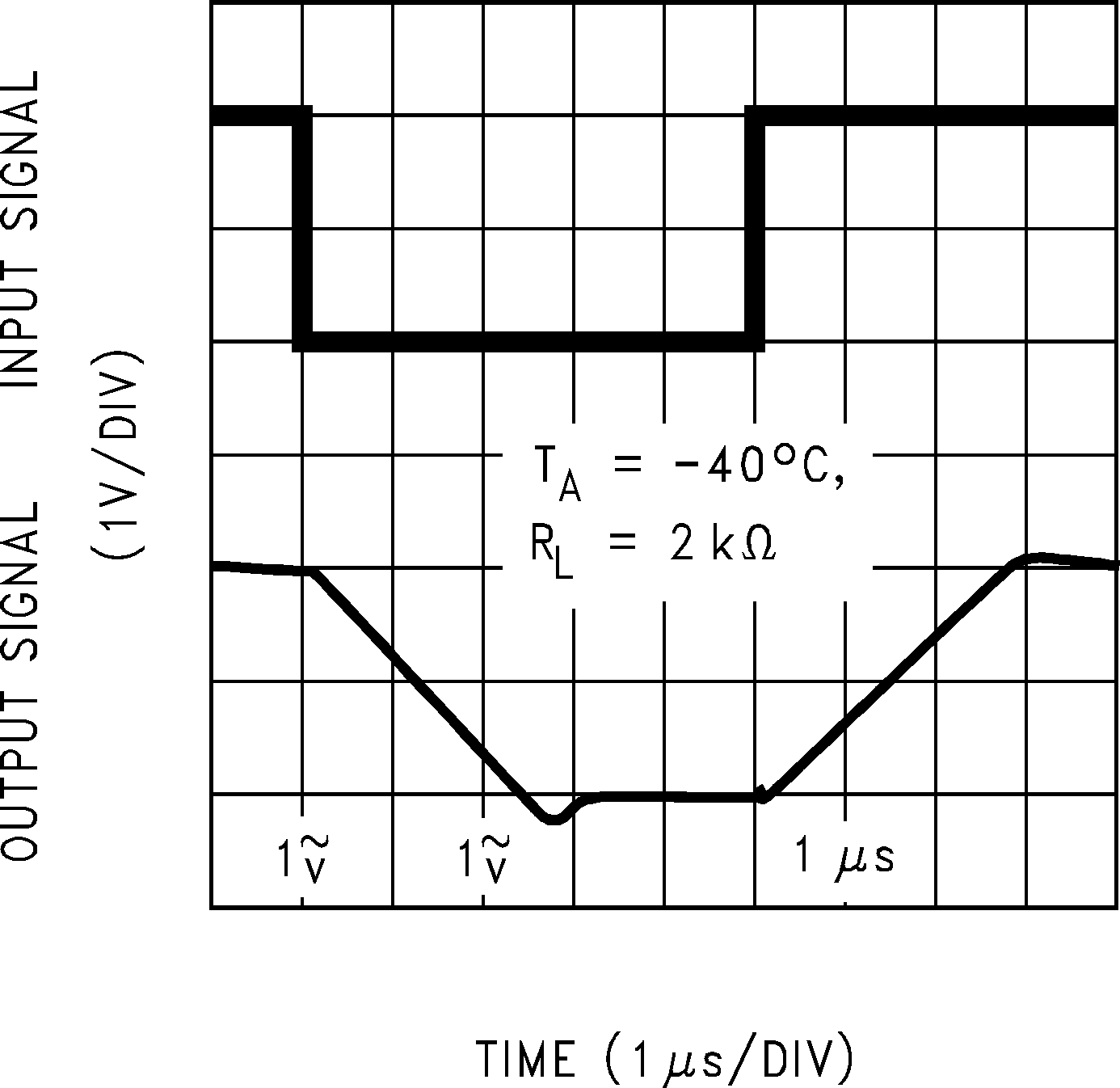 Figure 52. Noninverting Large Signal Pulse Response
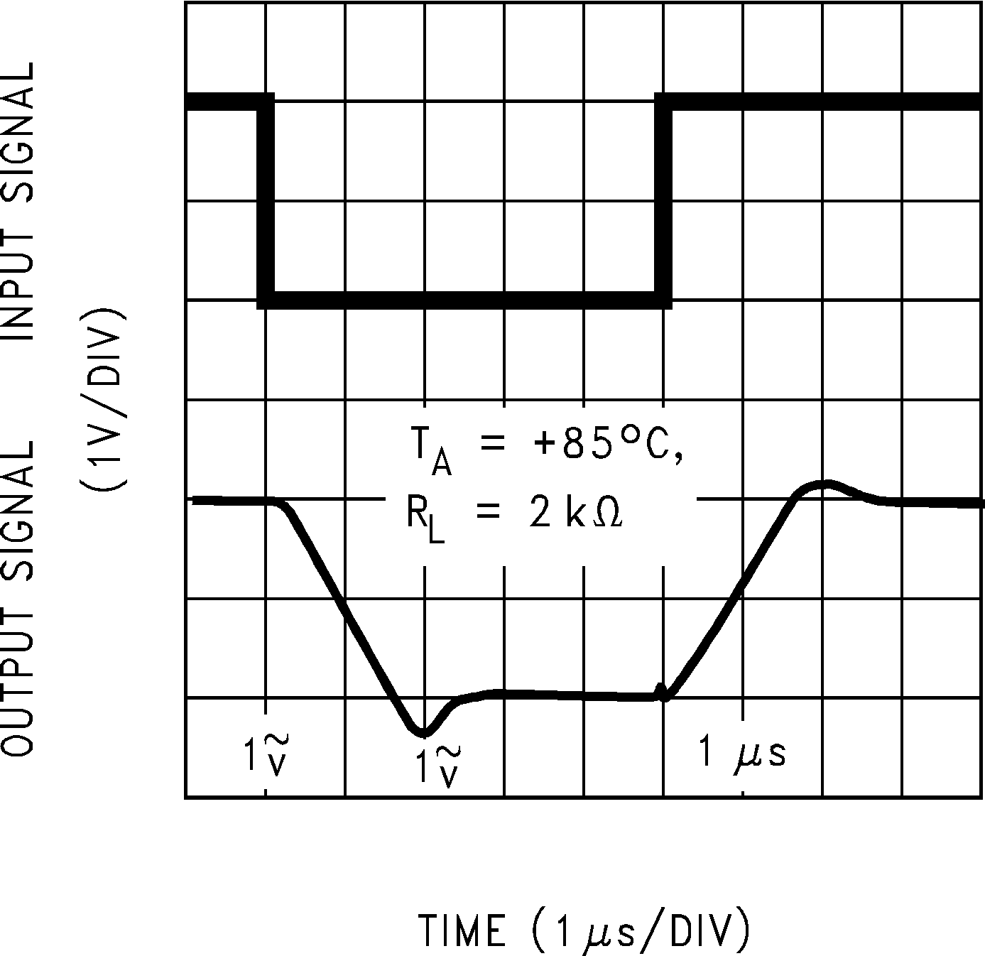 Figure 54. Noninverting Large Signal Pulse Response
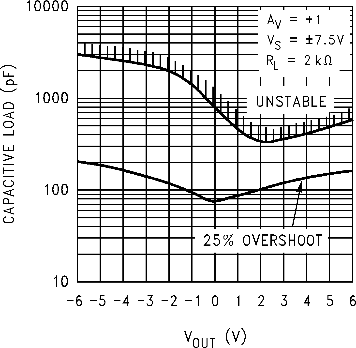 Figure 56. Stability vs Capacitive Load
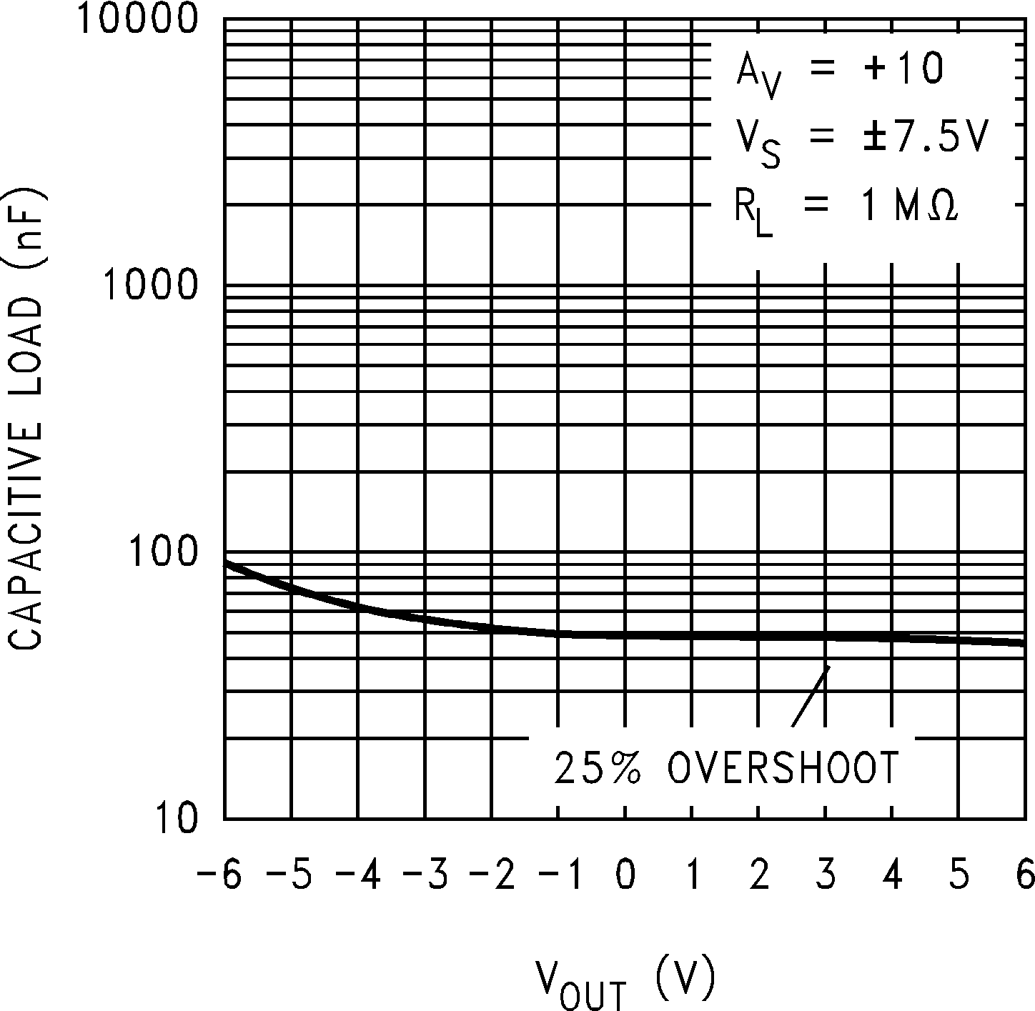 Figure 58. Stability vs Capacitive Load
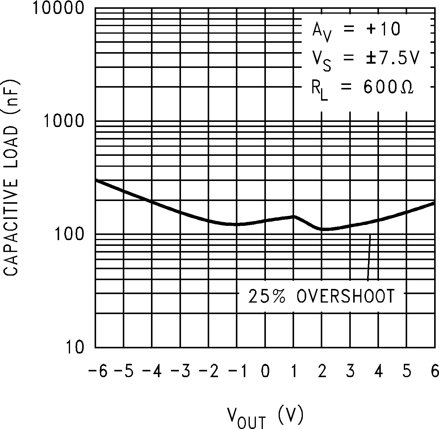 Figure 60. Stability vs Capacitive Load